Eureka AIR delivers breakthrough ideas for toughest innovation challenges, trusted by R&D personnel around the world.

Rework method for wafer level chip packaging bumps

A chip packaging and wafer-level technology, which is applied in the manufacture of electrical components, electrical solid-state devices, semiconductor/solid-state devices, etc., can solve problems such as high risk of wafer scrapping, high-risk abnormalities, and inability to meet SMT requirements

Active Publication Date: 2016-05-25
NANTONG FUJITSU MICROELECTRONICS
View PDF8 Cites 4 Cited by
  • Summary
  • Abstract
  • Description
  • Claims
  • Application Information

AI Technical Summary

Problems solved by technology

However, if the entire wafer is packaged, the risk of abnormal scrapping will be very high, such as figure 1 As shown, bump (bump) solder explosion, bridging, and deformation are one of the high-risk abnormalities
Among them, bump 11 has this kind of abnormality, which can no longer meet the requirements of SMT (Surface Mount Technology, surface mount technology) assembly process.

Method used


Image

  • Rework method for wafer level chip packaging bumps
  • Rework method for wafer level chip packaging bumps
  • Rework method for wafer level chip packaging bumps

Examples


Embodiment 1

[0031] A method for reworking wafer-level chip packaging bumps, comprising the following steps:

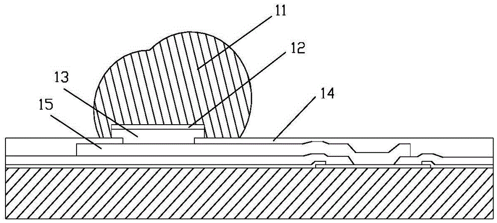
[0032] see figure 1 and figure 2 , (1) remove the bump: use the first wet etching solution to dissolve the bump 11 to form the surface solder attachment residue 16; the mass percentage of each substance in the first wet etching solution is: 15% nitric acid, 65% formazan cyclic acid, 20% pure water.

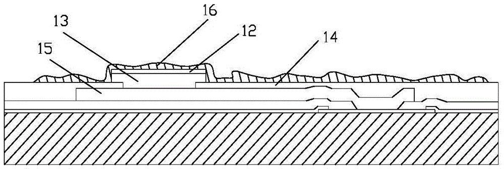
[0033] see figure 2 and image 3 , (2) Removal of surface solder adhesion residue 16: remove surface solder adhesion residue 16 by RF, Radio Frequency radio frequency back sputtering, after removing surface solder adhesion residue, expose bump solder 12 and passivation layer 14, bump pad 12 is provided with an IMC alloy layer 13; that is, only the bump pad 12 and the IMC alloy layer 13 are left at the original bump 11;

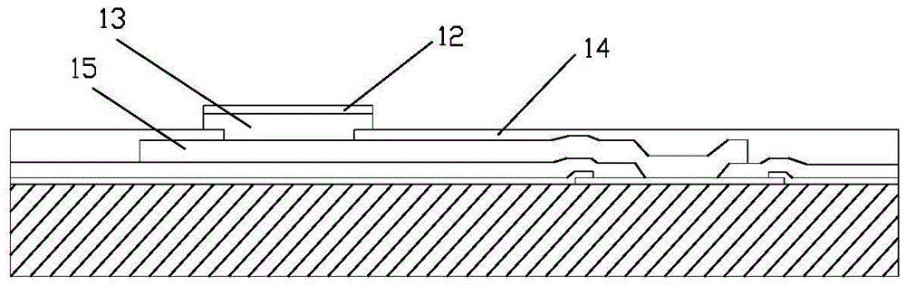
[0034] see image 3 and Figure 4 , (3) remove the bump pad 12 and the IMC alloy layer 13: carry out the copper etching of the bump pad by the second wet etc...

Embodiment 2

[0038] The method is the same as that of Example 1, except that the mass percentages of the substances in the first wet etching solution are: 10% nitric acid, 60% methyl cyclonic acid, and 30% pure water.

Embodiment 3

[0040] The method is the same as that of Example 1, except that the mass percentages of the substances in the first wet etching solution are: 12% nitric acid, 70% methyl cyclonic acid, and 18% pure water.


PUM


Abstract

The invention discloses a rework method for wafer level chip packaging bumps. The rework method comprises the following steps: (1) removing the bumps: carrying out bump dissolution by using a first wet process etching solution to form residues attached with soldering tin on the surfaces; (2) removing the residues attached with the soldering tin on the surfaces, wherein a lug bonding pad and a passivating layer are exposed after the residues attached with the soldering tin on the surfaces are removed, and an IMC alloy layer and an Intermetallic compound alloy layer are arranged below the lug bonding pad; (3) removing the lug bonding pad and the IMC alloy layer; and (4) removing 14, wherein obtained wafers are in the rewiring state of a redistribution layer. For the sake of no scrap and little yield loss for the wafers, the technique disclosed by the invention can remove bumps by using an etching technology, the wafers are recovered to an RDL rewiring state, and finally a processing flow is restarted.

Description

technical field [0001] The invention relates to the field of wafer packaging, in particular to a method for reworking bumps of wafer-level chip packaging. Background technique [0002] In recent years, the Wafer Level Chip Scale Packaging (WLCSP) process has been widely used. The volume of the chip packaged by this process is equivalent to the original size of the bare IC (integrated circuit, integrated circuit), which not only significantly reduces the size of the memory module, It meets the high-density requirements of mobile devices for the body space; on the other hand, in terms of performance, the speed and stability of data transmission are improved. In order to realize the WLCSP process, the entire wafer is packaged and tested in the process flow, and finally cut into individual IC particles. However, if the entire wafer is packaged, the risk of abnormal scrapping will be very high, such as figure 1 As shown, bump (bump) solder explosion, bridging, and deformation a...

Claims


Application Information

Patent Timeline
Patent Type & Authority Applications(China)
IPC IPC(8): H01L21/60
CPCH01L24/81H01L2224/81H01L2224/11
Inventor 钱泳亮
Owner NANTONG FUJITSU MICROELECTRONICS
Why Eureka
Eureka Blog
Learn More