Low-trigger-voltage SCR (semiconductor control rectifier) device used for ESD (electro-static discharge) protection

A low trigger voltage, ESD protection technology, applied in the direction of electric solid devices, electrical components, semiconductor devices, etc., can solve the problem of reducing the trigger voltage of SCR devices, and achieve the effect of reducing the trigger voltage

Active Publication Date: 2016-05-25
UNIV OF ELECTRONICS SCI & TECH OF CHINA
View PDF3 Cites 18 Cited by
  • Summary
  • Abstract
  • Description
  • Claims
  • Application Information

AI Technical Summary

Problems solved by technology

[0013] Although the existing LVTSCR (low voltage triggering SCR) device structure can reduce the trigger voltage of SCR devices, with the continuous improvement of process requirements, the trigger voltage of SCR devices has been further reduced.

Method used


Image

  • Low-trigger-voltage SCR (semiconductor control rectifier) device used for ESD (electro-static discharge) protection
  • Low-trigger-voltage SCR (semiconductor control rectifier) device used for ESD (electro-static discharge) protection
  • Low-trigger-voltage SCR (semiconductor control rectifier) device used for ESD (electro-static discharge) protection

Examples


Embodiment 1

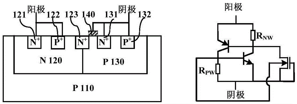
[0026] This embodiment provides a novel low trigger voltage SCR device, the structure and equivalent circuit of the SCR device are as follows figure 2 As shown, its structure includes:

[0027] p-type silicon substrate 110;

[0028] A well region is formed on the p-type silicon substrate 110, the well region includes an n-type well region 120 and a p-type well region 130, and the well region 120 is adjacent to the well region 130;

[0029] The n-type well region 120 is provided with an n-type heavily doped region 121 and a p-type doped region 122, and the n-type heavily doped region 121 and the p-type heavily doped region 122 are connected to the anode;

[0030] The p-type well region 130 is provided with an n-type heavily doped region 131 and a p-type heavily doped region 132, and the n-type heavily doped region 131 and the p-type heavily doped region 132 are connected to the cathode;

[0031] The n-type heavily doped region 123 is bridged between the n-type well region 12...

Embodiment 2

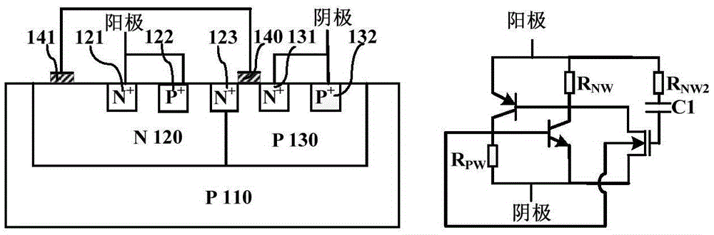
[0036] This embodiment provides a novel low trigger voltage SCR device, the structure and equivalent circuit of the SCR device are as follows image 3 As shown, in its structure, the gate oxide layer region 142 on the silicon surface of the n-type well region 120 is arranged between the p-type heavily doped region 122 and the n-type heavily doped region 123, and the surface of the gate oxide layer region 142 is a polysilicon layer It is connected to the polysilicon layer on the surface of the gate oxide region 140 through a metal layer.

[0037] The SCR device is composed of a parasitic PNP transistor, a parasitic NPN transistor and a parasitic N-channel MOSFET device. Among them, p-type heavily doped region 122, n-type well region 120, p-type well region 130 and p-type heavily doped region 132 form a PNP transistor; n-type heavily doped region 131, p-type well region 130, n-type Well region 120 and n-type heavily doped region 121 form an NPN transistor; n-type heavily doped ...

Embodiment 3

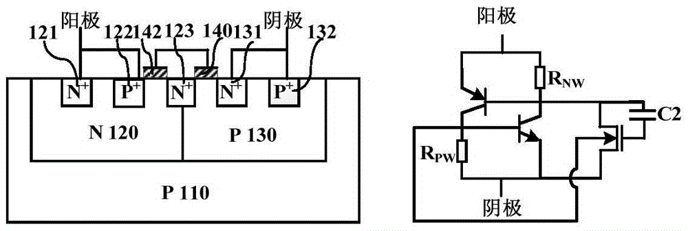
[0043] This embodiment provides a novel low trigger voltage SCR device. In the SCR device structure, the gate oxide region on the silicon surface of the n-type well region 120 is arranged in the n-type heavily doped region 121 close to the n-type well region and the p-type well region. The polysilicon layer on the surface of the gate oxide region is connected to the polysilicon layer on the surface of the gate oxide region 140 through a metal layer.

[0044] To sum up, the present invention provides a new type of low trigger voltage SCR device for ESD protection. Through the design of the internal structure, only a gate oxide layer structure is added on the basis of the existing LVTSCR device, and an RC is introduced inside the device. (Resistance-Capacity) path, without changing the area of ​​the device, the purpose of further reducing the trigger voltage of the SCR device is realized.


PUM


Abstract

The invention belongs to the electro-static discharge protection field for an integrated circuit, and provides a low-trigger-voltage SCR (semiconductor control rectifier) device used for ESD (electro-static discharge) protection used for further lowering the trigger voltage of an LVTSCR (low voltage triggering semiconductor control rectifier) device. The low-trigger-voltage SCR device comprises a first conductive type silicon substrate, a second conductive type well region and a first conductive type well region formed on the silicon substrate, wherein a second conductive type heavily-doped region and a first conductive type heavily-doped region are arranged in each well region separately; the second conductive type heavily-doped region is bridge jointed between the two well regions; a gate oxide layer region is arranged on the silicon surface between the bridge jointed second conductive type heavily-doped region, and the second conductive type heavily-doped region in the first conductive type well region; and the other gate oxide layer region is further arranged on a device-free structural region on the silicon surface in the second conductive type well region; and polysilicon layers on the two gate oxide layer regions are connected through metals. According to the low-trigger-voltage SCR device used for ESD protection, an RC (resistance-capacity) access is introduced into the device, so that the trigger voltage of the SCR device can be further lowered, and in addition, the trigger voltage can be modulated.

Description

technical field [0001] The invention belongs to the field of electrostatic discharge (ESD: Electro-Staticdischarge) protection of integrated circuits, relates to an ESD protection structure device, in particular to a novel silicon-controlled rectifier (SCR: Semiconductor Control Rectifier) ​​device for ESD protection with low trigger voltage structure. Background technique [0002] Electrostatic discharge is one of the important branches of integrated circuit reliability. Integrated circuits may be damaged by ESD during manufacturing, transportation and use. According to statistics, the economic losses caused by ESD in the semiconductor industry amount to billions of dollars every year, so it is of great significance to study the ESD protection of integrated circuits. [0003] In integrated circuits, diodes, MOSFETs, SCRs, etc. can be used as ESD protection devices, among which SCR is one of the most efficient ESD protection devices; SCR can withstand high ESD current due t...

Claims


Application Information

Patent Timeline
Patent Type & Authority Applications(China)
IPC IPC(8): H01L23/60H01L27/02
CPCH01L23/60H01L27/0296
Inventor 刘继芝赵柳刘志伟
Owner UNIV OF ELECTRONICS SCI & TECH OF CHINA
Why Eureka
Try Eureka