Package for semiconductor devices sensitive to mechanical and thermo-mechanical stresses, such as MEMS pressure sensors
A technology of semiconductors and devices, applied in the field of packaging of semiconductor devices, can solve problems such as the inability to use MEMS pressure sensors
- Summary
- Abstract
- Description
- Claims
- Application Information
AI Technical Summary
Problems solved by technology
Method used
Image
Examples
Embodiment Construction
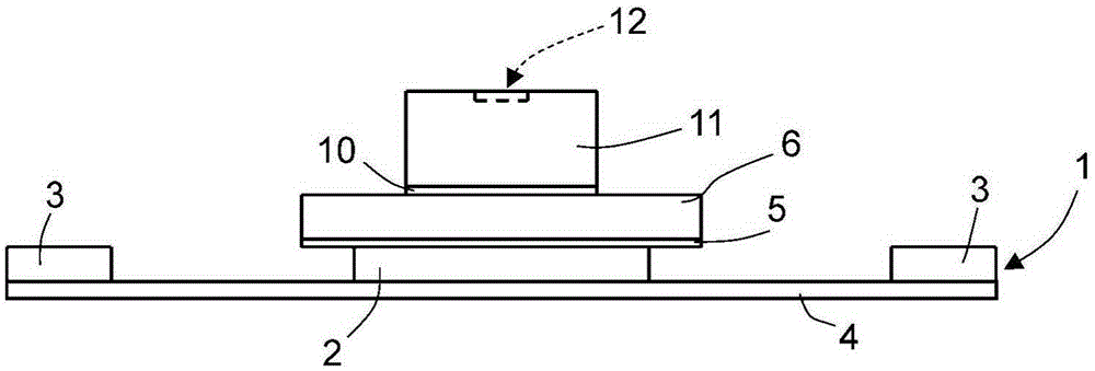
[0022] figure 1 A support frame 1 for a QFN (Quad Flat No-leads) package is shown comprising a die pad 2 attached on an adhesive tape 4 and a plurality of terminals 3 . The support frame 1 is a lead frame and may be made of any suitable material such as copper, aluminum and the like. In this embodiment, the die pad 2 is not plated on the bottom, while the terminals 3 are plated on the bottom and sides. For example, the terminals 3 may be Ni, Pd, Au or similar plated in a manner known per se for QFN packages. The adhesive strip 4 may be a thermoplastic standard adhesive strip attached to the rear side of the support frame 1 .
[0023] then, figure 2 , attach the first adhesive film 5 to the front surface of the die pad 2 and place the first die 6 on the first adhesive film 5 . The first die 6 is larger than the die pad 2 . The first adhesive layer 5 may be DAF (Die Attach Film) currently used in the semiconductor industry; known epoxy resins. The first adhesive film 5 ...
PUM
 Abstract
Description
Claims
Application Information


