Super-light resistive random access memory and preparation method thereof

A technology of resistive variable memory and silk protein, which is applied in the field of electronic technology and memory devices, can solve the problems of heavy resistance variable memory and lack of memory technology, and achieve the effects of no biological toxicity, less pollution, and simple operation

Inactive Publication Date: 2016-06-01
XIDIAN UNIV
View PDF4 Cites 13 Cited by
  • Summary
  • Abstract
  • Description
  • Claims
  • Application Information

AI Technical Summary

Problems solved by technology

In ultra-light wearable electronic products, medical health monitoring, robots, remote sensing and other systems, data storage devices are an essential part, but ultra-light memory technology is still relatively lacking.
Among many memory devices, resistive memory is considered to be the next-generation memory due to its advantages such as good scalability, high storage density, low power consumption, fast read and write speed, strong resistance to repeated operations, and long data retention time. One of the most powerful candidates, but the resistive memory of the existing technology is generally heavy

Method used


Image

  • Super-light resistive random access memory and preparation method thereof
  • Super-light resistive random access memory and preparation method thereof
  • Super-light resistive random access memory and preparation method thereof

Examples


preparation example Construction

[0028] A method for preparing an ultra-light resistive variable memory, comprising the following steps:

[0029] Step 1, growing a single-layer perfluorododecyltrichlorosilane film on a silicon substrate by chemical vapor phase method;

[0030] Step 2, growing a gold thin film electrode layer on the perfluorododecyltrichlorosilane layer, the thickness of the grown gold thin film electrode layer is 20-50 nanometers;

[0031] Step 3: On the electrode layer of the gold film, drop-coat the silk protein film. When drip-coating the silk protein film, use an aqueous solution of silk protein with a mass concentration of 1%-6%. After the drop-coating, place it in the atmosphere for 24 hours to dry naturally , the thickness of the formed silk protein film is 1-10 microns;

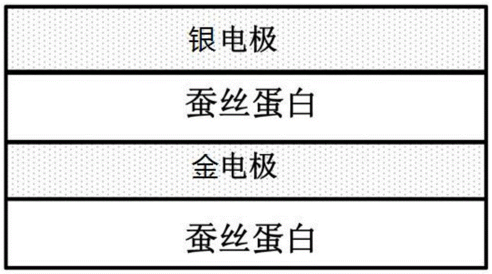
[0032] Step 4, peel off the silk protein film from the substrate substrate, during this process, the gold film electrode will be adhered to the silk protein film and be peeled off together, and the peeled silk prote...

Embodiment 1

[0036] Step 1, growing a single-layer perfluorododecyltrichlorosilane film on a silicon substrate by chemical vapor phase method;

[0037] Step 2, growing a gold thin film electrode layer on the perfluorododecyltrichlorosilane layer, the thickness of the grown gold thin film electrode layer is 50 nanometers;

[0038] Step 3: On the electrode layer of the gold film, drop-coat the silk protein film. When drip-coating the silk protein film, use an aqueous solution of silk protein with a mass concentration of 1%-6%. After the drop-coating, place it in the atmosphere for 24 hours to dry naturally , the thickness of the formed fibroin film is 10 microns;

[0039] Step 4, peel off the silk protein film from the substrate substrate, during this process, the gold film electrode will be adhered to the silk protein film and be peeled off together, and the peeled silk protein film will be adhered to the supporting substrate, where the gold The surface of the thin film electrode is upward...

Embodiment 2

[0044] Step 1, growing a single-layer perfluorododecyltrichlorosilane film on a silicon substrate by chemical vapor phase method;

[0045] Step 2, growing a gold thin film electrode layer on the perfluorododecyltrichlorosilane layer, the thickness of the grown gold thin film electrode layer is 20 nanometers;

[0046] Step 3, drip-coat silk protein film on the gold film electrode layer. When drip-coating the silk protein film, use an aqueous solution of silk protein with a mass concentration of 1%. After drip-coating, place it in the atmosphere for 24 hours to dry naturally, and the formed The thickness of the silk protein film is 1 micron;

[0047] Step 4, peel off the silk protein film from the substrate substrate, during this process, the gold film electrode will be adhered to the silk protein film and be peeled off together, and the peeled silk protein film will be adhered to the supporting substrate, where the gold The surface of the thin film electrode is upward;

[004...


PUM

PropertyMeasurementUnit
thicknessaaaaaaaaaa
thicknessaaaaaaaaaa
thicknessaaaaaaaaaa

Abstract

The invention discloses a super-light resistive random access memory and a preparation method thereof. The super-light resistive random access memory comprises a metal thin-film electrode; a first silk protein film and a second silk protein film cover an upper layer and a lower layer of the metal thin-film electrode respectively; and a silver thin-film electrode covers the first silk protein film. The light silk protein is used as a substrate and is also used as a resistive material, so that the resistive random access memory with the mass per unit area of 4mg/cm<2> can be obtained; and the mass per unit area of the resistive random access memory is smaller than that of the silicon-substrate-based traditional resistive random access memory by over 320 times and is smaller than that of the common A4 paper by over 20 times.

Description

【Technical field】 [0001] The invention belongs to the field of electronic technology and memory devices, and in particular relates to an ultra-light resistive variable memory and a preparation method thereof. 【Background technique】 [0002] With the continuous advancement of electronic information technology, there is an increasing demand for light weight and portable electronic products. In the past two years, the development of ultra-light electronic devices has received extensive attention. For example: Professor TakaoSomeya of the University of Tokyo and his collaborators proposed that the quality of the preparation on the plastic substrate is only 3g / m 2 The organic thin film transistor and its mass is only 4g / m 2 methods for organic solar cells, etc. Ultra-lightweight electronic devices have broad application prospects in wearable electronic products, medical health monitoring, robotics, remote sensing and other fields. Electronic devices such as ultra-light thin f...

Claims


Application Information

Patent Timeline
Patent Type & Authority Applications(China)
IPC IPC(8): H01L27/28H01L51/56
CPCH10K19/10H10K71/12
Inventor 王宏马晓华郝跃
Owner XIDIAN UNIV
Why Eureka
Try Eureka