Nitride light emitting diode with AIN quantum dots and manufacturing method thereof

A technology of light-emitting diodes and manufacturing methods, which is applied in the direction of electrical components, circuits, semiconductor devices, etc., can solve problems such as leakage and ESD deviation, and achieve the effects of increasing reverse voltage, reducing leakage, and preventing current from flowing through the dislocation line area

Active Publication Date: 2016-06-01
XIAMEN SANAN OPTOELECTRONICS TECH CO LTD
View PDF7 Cites 8 Cited by
  • Summary
  • Abstract
  • Description
  • Claims
  • Application Information

AI Technical Summary

Problems solved by technology

Nitride light-emitting diodes are generally epitaxial on heterogeneous substrates. Due to lattice mismatch and thermal mismatch, a large number of dislocations and defects will be generated. Although some dislocations can be reduced by structural design, there ar

Method used


Image

  • Nitride light emitting diode with AIN quantum dots and manufacturing method thereof
  • Nitride light emitting diode with AIN quantum dots and manufacturing method thereof
  • Nitride light emitting diode with AIN quantum dots and manufacturing method thereof

Examples


Embodiment Construction

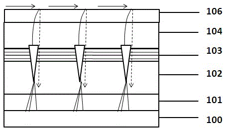
[0018] Such as figure 1 As shown, a conventional nitride light-emitting diode sequentially includes a substrate 100, a buffer layer 101, an N-type nitride 102, a multiple quantum well 103 with V-pits, a P-type nitride 104, and a P-type contact layer 106. A large number of dislocations caused by lattice mismatch and thermal mismatch will extend to the P-type layer to form a leakage channel, and electrons will tend to flow to the dislocation line with lower resistance, reducing the lateral expansion of the current, resulting in EDS deviation and leakage.

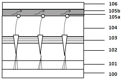
[0019] Such as figure 2 As shown, a light-emitting diode with AlN quantum dots proposed by the present invention sequentially includes a substrate 100, a buffer layer 101, an N-type nitride 102, a multiple quantum well 103 with V-pits, a P-type nitride 104, and no Mg-doped AlN quantum dots 105a, P-type nitride 105b with high Mg doping, and P-type contact layer 106, wherein there is no Mg inserted between the P-type nitride a...


PUM


Abstract

The present invention discloses a nitride light emitting diode with AIN quantum dots and a manufacturing method thereof. The nitride light emitting diode comprises a substrate, a buffer layer, an N-type nitride, multiple quantum wells with V-pits, P-type nitride, AIN quantum dots without Mg doping and P-type nitride and P-type contact layer with high Mg doping, an AIN quantum dot layer is inserted between the P-type nitride and the P-type nitride with high Mg doping, and the quantum dots uniformly block the terminal of a dislocation line through a multistep relaxation deposition method with high-resistance AIN quantum dots. The nitride light emitting diode with AIN quantum dots and the manufacturing method thereof are able to prevent current from flowing the dislocation line area, improve the backward voltage, reduce the electric leakage and improve the current lateral extension and ESD.

Description

technical field [0001] The invention relates to the field of semiconductor optoelectronic devices, in particular to a nitride light-emitting diode with AlN quantum dots and a manufacturing method thereof. Background technique [0002] Nowadays, light-emitting diodes (LEDs), especially nitride light-emitting diodes, have been widely used in the field of general lighting due to their high luminous efficiency. Nitride light-emitting diodes are generally epitaxial on heterogeneous substrates. Due to lattice mismatch and thermal mismatch, a large number of dislocations and defects will be generated. Although some dislocations can be reduced by structural design, there are still a large number of dislocations that will extend When the P-type layer forms a leakage channel, electrons will tend to flow to the dislocation line with lower resistance, reducing the lateral expansion of the current, resulting in ESD deviation and leakage. [0003] In view of the performance problems of t...

Claims


Application Information

Patent Timeline
IPC IPC(8): H01L33/06H01L33/00H01L33/32
CPCH01L33/0075H01L33/06H01L33/32
Inventor 郑锦坚钟志白杜伟华李志明杨焕荣廖树涛伍明跃周启伦林峰李水清康俊勇
Owner XIAMEN SANAN OPTOELECTRONICS TECH CO LTD
Why Eureka
Try Eureka