Iii-v semiconductor pixel x-ray detector

a pixel x-ray and semiconductor technology, applied in the direction of semiconductor devices, electrical equipment, radio frequency control devices, etc., can solve the problems of residual or leakage current, junctions or mesa structures, and disadvantages of described structures, and achieve low blocking current, high reverse voltage, and high breakdown voltage

Active Publication Date: 2021-09-23
AZUR SPACE SOLAR POWER
View PDF2 Cites 1 Cited by
  • Summary
  • Abstract
  • Description
  • Claims
  • Application Information

AI Technical Summary

Benefits of technology

[0051]The advantages of the semiconductor detector according to the invention are a particularly low blocking current and a high breakdown voltage. In particular, the breakdown characteristic has a nearly ideal profile. The particularly low blocking current permits the application of high reverse voltages, whereby a very high sensitivity is reached.
[0052]The breakdown voltage can also be determined by the minimum distance between the semiconductor passivation layer and the semiconductor contact regions. The X-ray detector according to the invention makes it possible to achieve disruptive field strengths of up to 40 V / μm and extremely reliable disruptive field strengths of more than 30 V / μLm.
[0053]III-V materials, in particular GaAs, additionally permit a particularly sensitive or efficient detection of X-rays, in particular low-energy X-rays, due to a high charge carrier mobility.
[0054]An advantage of the X-ray detector according to the invention is therefore the great sensitivity, whereby a reduction of the necessary dose to which a patient, for example, must be exposed, is possible.
[0055]Due to the high mobility of the charge carriers, only a very short time per image recording is likewise needed, which results in a low radiation exposure. Moreover, the high charge carrier mobility allows color X-rays to be taken, based on photon counting.
[0056]The component according to the invention is also able to be manufactured in comparatively few process steps and thereby relatively cost-effectively or at least at reasonable cost.

Problems solved by technology

The residual or leakage currents, which occur during an operation in the non-conducting direction, in particular via the edges of the planar p-n junctions or the mesa structures, are a disadvantage of the described structures.

Method used


Image

  • Iii-v semiconductor pixel x-ray detector
  • Iii-v semiconductor pixel x-ray detector
  • Iii-v semiconductor pixel x-ray detector

Examples


Embodiment Construction

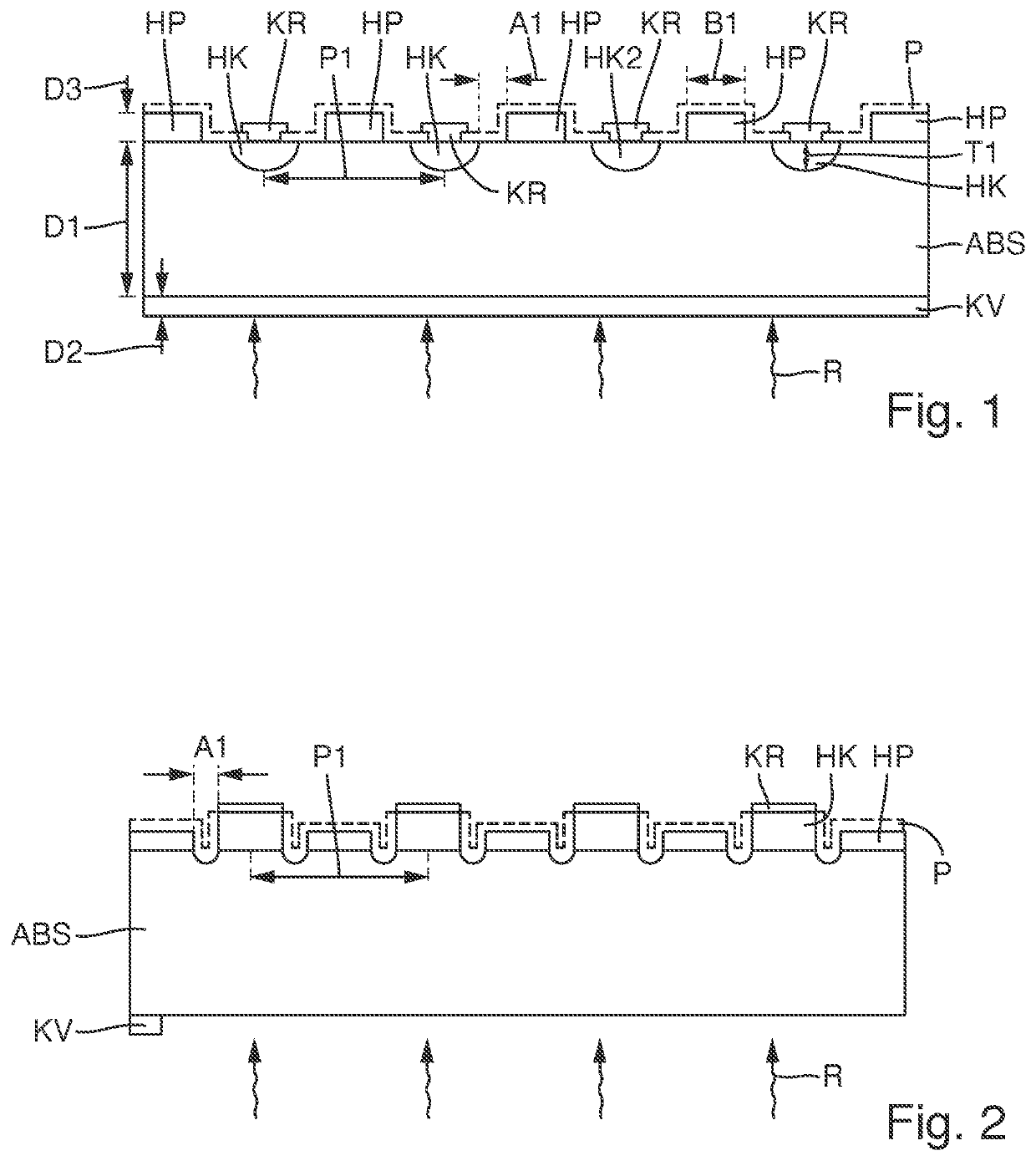
[0080]The illustration in FIG. 1 shows a cross-section of a first specific embodiment according to the invention of a III-V semiconductor pixel X-ray detector for detecting X-rays R.

[0081]The X-ray detector has a matrix of four by four III-V semiconductor pixels. It should be noted that, in a specific embodiment which is not illustrated, the array has three by three III-V semiconductor pixels. It is understood that, in another specific embodiment which is not illustrated, the X-ray detector has more than sixteen III-V semiconductor pixels.

[0082]The semiconductor pixels comprise a common absorption region ABS, including an underside, an upper side and a layer thickness D1, as well as a common front side connecting contact KV, the front side connecting contact being designed as a metal layer having a preferably limited layer thickness D2, and the underside of absorption region ABS being covered and integrally connected to the underside of absorption region ABS.

[0083]Each semiconductor...


PUM

PropertyMeasurementUnit
distanceaaaaaaaaaa
distanceaaaaaaaaaa
distanceaaaaaaaaaa

Abstract

A III-V semiconductor pixel X-ray detector, including an absorption region of a first or a second conductivity type, at least nine semiconductor contact regions of the second conductivity type arranged in a matrix along the upper side of the absorption region, and optionally a semiconductor contact layer of the first conductivity type, a metallic front side connecting contact being arranged beneath the absorption region, and a metallic rear side connecting contact being arranged above each semiconductor contact region, and a semiconductor passivation layer of the first or the second conductivity type. The semiconductor passivation layer and the absorption region being lattice-matched to each other. The semiconductor passivation layer being arranged in regions on the upper side of the absorption region. The semiconductor passivation layer having a minimum distance of at least 2 μm or at least 20 μm with respect to each highly doped semiconductor contact region.

Description

[0001]This nonprovisional application claims priority under 35 U.S.C. § 119(a) to German Patent Application No. 10 2020 001 839.4, which was filed in Germany on Mar. 20, 2020 and which is herein incorporated by reference.BACKGROUND OF THE INVENTIONField of the Invention[0002]The present invention relates to III-V semiconductor pixel X-ray detector.Description of the Background Art[0003]A method and a device for manufacturing a GaAs detector for detecting X-rays and an imaging are known from “A Method for Adjusting the Performance of Epitaxial GaAs X-Ray Detectors,” Sun, G. C. and Bourgoin, J. C., Nucl. Instrum. Methods Phys. Res., Sect. A, 2003, vol. 512, pp. 355-360, from “GaAs Schottky Versus p / i / n Diodes for Pixelated X-Ray Detectors”, Bourgoin, J. C. and Sun, G. C., Nucl. Instrum. Methods Phys. Res., Sect. A, 2002, vol. 487, pp. 47-49, likewise from DE 602 21 638 T2.[0004]Another GaAs imaging device for detecting X-rays is furthermore known from WO 2004 816 04 A2.[0005]P-i-n str...

Claims


Application Information

Patent Timeline
Patent Type & Authority Applications(United States)
IPC IPC(8): H01L27/146G01T1/24
CPCH01L27/14659G01T1/24H01L27/14676H01L27/14605
Inventor STROBL, GERHARD
Owner AZUR SPACE SOLAR POWER
Why Eureka
Try Eureka