Control method for uniformly laminating multi-layered PCB

A control method and PCB board technology, which is applied in multilayer circuit manufacturing, printed circuit manufacturing, electrical components, etc., can solve the problem of reduced pressure and temperature uniformity of the hot plate of the press, poor uniformity of the PCB board, and poor overall uniformity of the board and other problems to achieve the effect of optimizing pressing parameters, avoiding poor pressing uniformity, and low cost

Active Publication Date: 2016-06-01
AOSHIKANG TECH CO LTD
View PDF3 Cites 25 Cited by
  • Summary
  • Abstract
  • Description
  • Claims
  • Application Information

AI Technical Summary

Problems solved by technology

[0003] At present, in the lamination process of PCB boards, due to the diversification of PCB product designs, such as: large layout, thick bottom copper, fine impedance, instability of raw materials, and occasional errors in the operation of employees, it is easy to cause the PCB after lamination The overall uniformity of the board is not good, and after the press has been used for a period of time, the pressure and temperature uniformity of the hot plate of the press will decrease, which will easily lead to abnormal pressing quality, large equipment wear and tear, reducing production efficiency, affecting product quality, and improving production efficiency. Cost of production
[0004] In addition, when the PCB board is pressed, the heating rate is between 2°C-3°C / Min; the high-pressure pressure is set at about 350Psi-480Psi, which will easily lead to shortening the time period of the resin in the prepreg being in the molten flow during the pressing process, resulting in filling And the flow is insufficient, the overall uniformity of the board after lamination is poor, especially when the inner layer has a thick bottom copper (≥2OZ) or thin Core (≤4mil) design or large typesetting (≥20inchx24inch) layout, no copper area position , the abnormality of the uniformity quality of the board edge and the board is more obvious

Method used


Image

  • Control method for uniformly laminating multi-layered PCB
  • Control method for uniformly laminating multi-layered PCB
  • Control method for uniformly laminating multi-layered PCB

Examples


Embodiment 1

[0036] This embodiment includes the following steps:

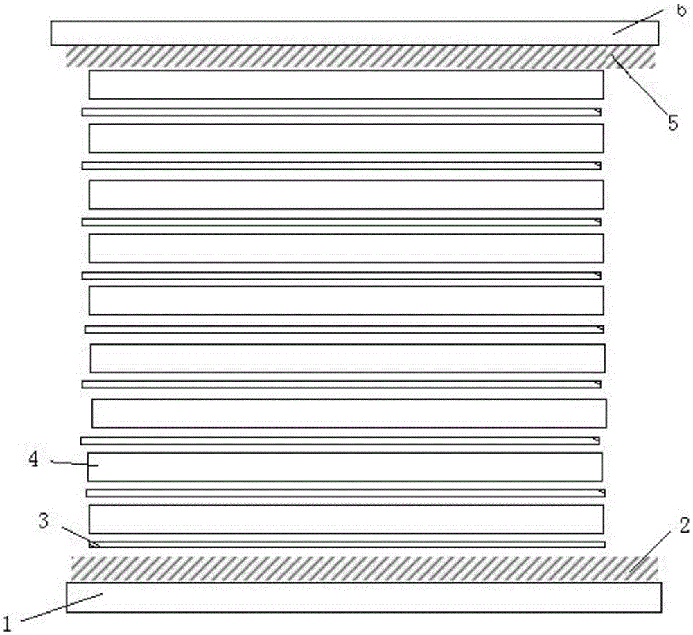
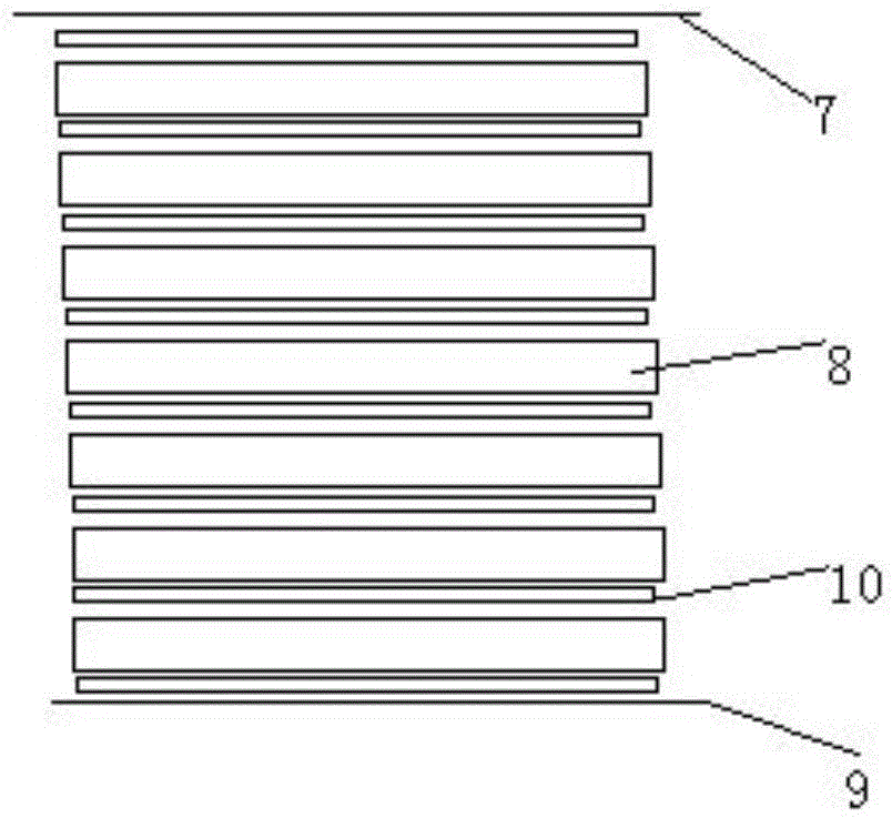
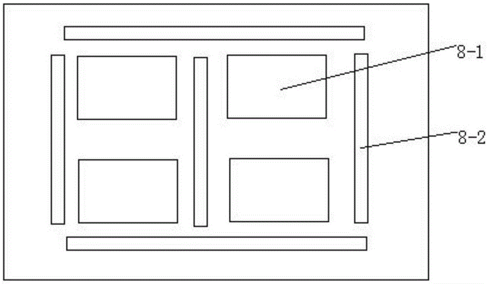
[0037] (1) PCB board stack: first place the carrier plate 1, place the lower buffer layer 2 on the carrier plate 1, place mirror steel plates 3 and PCB boards 4 alternately on the lower buffer layer 2, and the PCB board 4 is made of The upper copper foil 7, several core board layers 8 and the lower copper foil 9 are placed sequentially from top to bottom, and a prepreg 10 is placed between the upper copper foil 7 and the lower copper foil 9 and the adjacent core board layer 8, A prepreg 10 is placed between the core layer 8 and the core layer 8, and the placement positions of the core layer 8 and the prepreg 10 are positioned by an infrared positioning transmitter, and the number of the mirror steel plate 3 is the same as that of the PCB board 4 , the number of PCB boards 4 is adapted to the opening height of the hot plate of the pressing device, and then an upper buffer layer 5 is placed, and a cover plate 6 is placed abo...

Embodiment 2

[0052] This embodiment includes the following steps:

[0053] (2) PCB board stack: first place the carrier plate 1, place the lower buffer layer 2 on the carrier plate 1, and alternately place mirror steel plates 3 and PCB boards 4 on the lower buffer layer 2, and the PCB board 4 is made of The upper copper foil 7, several core board layers 8 and the lower copper foil 9 are placed sequentially from top to bottom, and a prepreg 10 is placed between the upper copper foil 7 and the lower copper foil 9 and the adjacent core board layer 8, A prepreg 10 is placed between the core layer 8 and the core layer 8, and the placement positions of the core layer 8 and the prepreg 10 are positioned by an infrared positioning transmitter, and the number of the mirror steel plate 3 is the same as that of the PCB board 4 , the number of PCB boards 4 is adapted to the opening height of the hot plate of the pressing device, and then an upper buffer layer 5 is placed, and a cover plate 6 is placed...


PUM


Abstract

A control method for uniformly laminating a multi-layered PCB is disclosed. The control method comprises the steps of PCB laminating and pressing. The control method is simple, convenient, and easy to operate and master; the layers are aligned accurately and the PCB is pressed uniformly; board sliding and decompression can be avoided, and high product quality can be achieved; the lamination process is easy to control, and easy machining and low cost are realized as well; the relatively consistent uniformity of the thickness of each laminated board among different layers can be accurately ensured; sufficient and uniform flowing adhesive in all directions is supplied; the thickness and the impedance of a laminated dielectric layer are moderate; the board edge is designed in a choked-flow manner; the overall uniformity of the laminated PCB is high; the fused flowing time of resin in a prepreg is prolonged, so that sufficient stuffing among the multiple core plate layers is ensured, uniform fused resin flowing is realized, and the efficiency is greatly improved; and in addition, the service life of equipment is prolonged, the lamination quality is effectively ensured, and the production cost is lowered.

Description

technical field [0001] The invention relates to the field of PCB board production and processing, in particular to a method for controlling uniform lamination of multilayer PCBs. Background technique [0002] PCB board, also known as printed circuit board, printed circuit board, referred to as printed board, is based on an insulating board, cut to a certain size, with at least one conductive pattern attached to it, and holes (such as component holes, fastening holes, metallized holes, etc.), and realize the interconnection between electronic components. Since such boards are made using electronic printing, they are called "printed" circuit boards. During the PCB manufacturing process, a multi-layer PCB is formed by using a prepreg to bond the various layers together under high temperature and pressure. The core board is the part that bears the graphics, and the core boards of different levels are bonded together by the adhesive sheet, and finally the finished printed circu...

Claims


Application Information

Patent Timeline
Patent Type & Authority Applications(China)
IPC IPC(8): H05K3/46
CPCH05K3/4638H05K2203/068
Inventor 刘君华程涌贺文辉龚德勋彭龙华
Owner AOSHIKANG TECH CO LTD
Why Eureka
Try Eureka