A CMOS Device Anti-Single Event Lockup Reinforcement Method

An anti-single particle and device technology, applied in the direction of single semiconductor device testing, semiconductor/solid-state device manufacturing, electrical components, etc., to achieve the effect of simple steps, shortened research and development cycle, and reduced cost

Active Publication Date: 2018-06-26
NORTHWEST INST OF NUCLEAR TECH
View PDF7 Cites 0 Cited by
  • Summary
  • Abstract
  • Description
  • Claims
  • Application Information

AI Technical Summary

Problems solved by technology

Therefore, not suitable for commercial CMOS devices

Method used


Image

  • A CMOS Device Anti-Single Event Lockup Reinforcement Method
  • A CMOS Device Anti-Single Event Lockup Reinforcement Method
  • A CMOS Device Anti-Single Event Lockup Reinforcement Method

Examples


Embodiment Construction

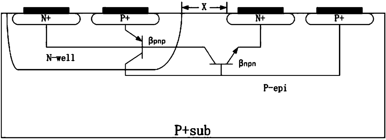
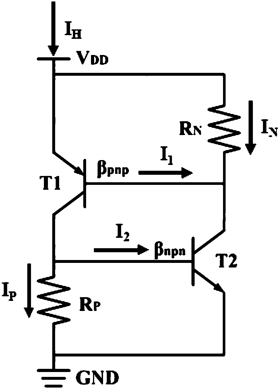
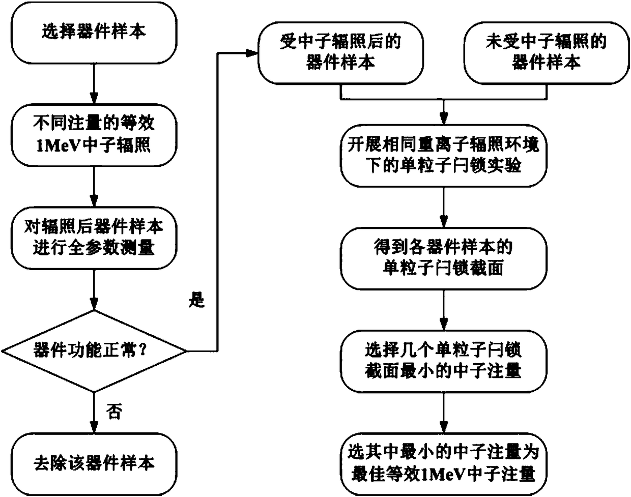
[0036] The neutron pre-irradiation reinforcement scheme proposed by the present invention has a wider application range, not only for military-grade and aerospace-grade CMOS devices, but also for commercial CMOS devices. Many studies at home and abroad have verified the influence of neutron irradiation on the DC current gain of bipolar devices. However, there is no method of applying neutron irradiation to device reinforcement in China, and foreign countries only use neutron irradiation for single The particle effect research has not actually been applied to device reinforcement. The present invention is based on the increasingly urgent application requirements of commercial CMOS devices in small satellites, and the anti-neutron radiation capability of modern CMOS devices can generally reach 110 15 n / cm 2 Above, this invention provides a feasibility guarantee. In addition, the present invention is aimed at the reinforcement of commercial CMOS devices for small satellites, so th...


PUM


Abstract

The invention discloses a reinforcement method for the single event latchup resistance of a CMOS device. Neutron irradiation is carried out on the CMOS device; a displacement damage is introduced in the neutron irradiation; and a current gain of a parasitical bipolar transistor in an inverter of the CMOS device is reduced, so that P-N-P-N latchup is not generated. The reinforcement method is an external reinforcement method; processing steps to produce the device will not be increased; there is no need to redesign a device layout for the single event latchup effect; and complexity of an original system will not be increased. Thus, the fixed size of the device will not be changed, and a peripheral circuit will not be increased either.

Description

Technical field [0001] The invention relates to a method for strengthening the anti-single-particle blocking of CMOS devices, and is especially suitable for strengthening the anti-single-particle blocking of commercial CMOS devices. technical background [0002] As an important research direction in the current aerospace field, small satellites are of great significance to national defense construction. In order to reduce R&D costs, reduce quality, and shorten the R&D cycle, the use of commercial CMOS devices in small satellites is a new development direction for aerospace technology. [0003] Commercial CMOS devices refer to off-the-shelf devices that can be purchased directly from the market. It has two meanings: one is that the product is of commercial or industrial grade to distinguish it from military and aerospace grades; the other is that the product is available from stock. No special customization is required. Currently, developed countries impose export restrictions on ...

Claims


Application Information

Patent Timeline
Patent Type & Authority Patents(China)
IPC IPC(8): H01L21/263G01R31/26
CPCG01R31/26H01L21/263
Inventor 郭红霞潘霄宇罗尹虹丁李利张凤祁魏佳男赵雯王园明刘玉辉
Owner NORTHWEST INST OF NUCLEAR TECH
Why Eureka
Try Eureka