Thin film transistor and preparation method therefor, and array substrate

A thin film transistor and carbon nanotube technology, applied in transistors, semiconductor/solid-state device manufacturing, semiconductor devices, etc., to achieve the effect of improving stability and avoiding adverse effects

Inactive Publication Date: 2016-06-15
BOE TECH GRP CO LTD +1
View PDF3 Cites 12 Cited by
  • Summary
  • Abstract
  • Description
  • Claims
  • Application Information

AI Technical Summary

Problems solved by technology

However, a preparation method that can avoid these problems has not been found so far. Therefore, the preparation technology of carbon nanotube bottom-gate thin film transistors needs further exploration.

Method used


Image

  • Thin film transistor and preparation method therefor, and array substrate
  • Thin film transistor and preparation method therefor, and array substrate
  • Thin film transistor and preparation method therefor, and array substrate

Examples


preparation example Construction

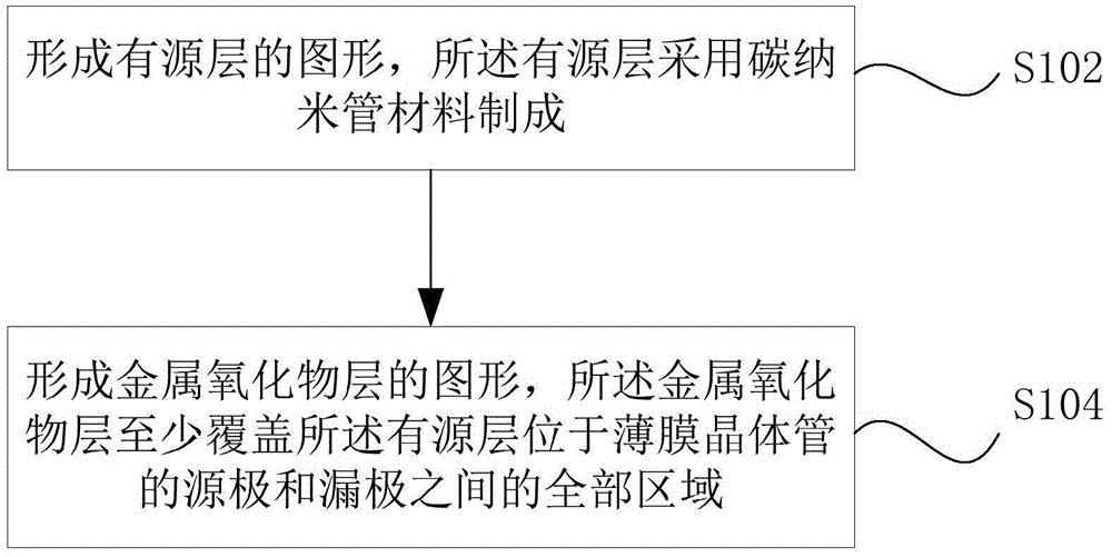
[0026] Based on this, an embodiment of the present invention provides a method for manufacturing a thin film transistor. figure 1 is a flow chart of a method for preparing a thin film transistor according to an embodiment of the present invention, such as figure 1 As shown, the process includes the following steps (step S102-step S104):

[0027] Step S102, forming the pattern of the active layer, the active layer is made of carbon nanotube material;

[0028] Step S104 , forming a pattern of a metal oxide layer, the metal oxide layer covering at least the entire area of ​​the active layer between the source and the drain of the thin film transistor.

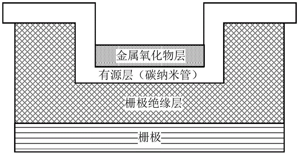
[0029] For the process of preparing the thin film transistor, firstly, a gate can be formed on a glass substrate, then a gate insulating layer can be formed on the gate, and then the pattern of the active layer can be formed on the gate insulating layer by using carbon nanotube material, and then Form the metal oxide layer and t...


PUM

PropertyMeasurementUnit
thicknessaaaaaaaaaa
thicknessaaaaaaaaaa

Abstract

The invention discloses a carbon nanotube bottom-gate thin film transistor and a preparation method therefor, and an array substrate. The preparation method for the carbon nanotube bottom-gate thin film transistor comprises the steps of forming an active layer pattern, wherein the active layer is made from a carbon nanotube material; and forming a metal oxide layer pattern, wherein the metal oxide layer at least covers all the regions, positioned between the source electrode and the drain electrode of the thin film transistor, of the active layer. By adoption of the carbon nanotube bottom-gate thin film transistor and the preparation method therefor, and the array substrate, an effect of improving the stability, reliability, mobility ratio and the like of the carbon nanotube bottom-gate thin film transistor is achieved.

Description

technical field [0001] The invention relates to the field of display technology, in particular to a thin film transistor, a preparation method thereof, and an array substrate. Background technique [0002] Single-wall semiconducting carbon nanotubes have broad application prospects in the fields of logic circuits and optoelectronic devices due to their excellent electrical and mechanical properties, such as field effect transistors, inverters, ring oscillators, and light-emitting devices. The synthesis methods of single-walled carbon nanotubes mainly include chemical vapor deposition, arc discharge and laser ablation, etc. The synthesized carbon nanotubes contain 2 / 3 semiconducting carbon nanotubes and 1 / 3 metallic carbon nanotubes. At present, the methods for purifying semiconducting carbon nanotubes mainly include gel method, density gradient centrifugation method and polymer selective dispersion method. Although single-wall semiconducting carbon nanotubes with high purity...

Claims


Application Information

Patent Timeline
Patent Type & Authority Applications(China)
IPC IPC(8): H01L21/336H01L29/786H01L27/12
CPCH01L27/1214H01L29/66742H01L29/7869H01L27/12H01L29/78684H10K85/221H10K10/472H10K10/484H10K10/88H10K10/84H10K10/466H10K19/10H10K71/211H10K2102/00
Inventor 梁学磊惠官宝夏继业张方振田博元严秋平彭练矛
Owner BOE TECH GRP CO LTD
Why Eureka
Try Eureka