Three-dimensional semiconductor device and production method of three-dimensional semiconductor device

A device manufacturing method and semiconductor technology, applied in the direction of semiconductor devices, electrical solid devices, electrical components, etc., can solve the problems of erasing holes and programming electron neutralization, and achieve the effect of improving data retention characteristics

Active Publication Date: 2016-06-15
INST OF MICROELECTRONICS CHINESE ACAD OF SCI
View PDF5 Cites 40 Cited by
  • Summary
  • Abstract
  • Description
  • Claims
  • Application Information

AI Technical Summary

Problems solved by technology

In addition, the charges accumulated in the storage layer will not only diffuse to the direction of the gate directly corresponding to it, but also further diffuse to the charge storage region corresponding to the adjacent (along the channel distribution direction, that is, the vertical direction) gate, cause unnecessary neutralization between erase holes and program electrons, resulting in figure 2 Larger Vt drift shown in the middle ①+② curve

Method used


Image

  • Three-dimensional semiconductor device and production method of three-dimensional semiconductor device
  • Three-dimensional semiconductor device and production method of three-dimensional semiconductor device
  • Three-dimensional semiconductor device and production method of three-dimensional semiconductor device

Examples


Embodiment Construction

[0023] The features and technical effects of the technical solution of the present invention will be described in detail below with reference to the accompanying drawings and in conjunction with exemplary embodiments, and a semiconductor storage device and a manufacturing method thereof that effectively improve data retention characteristics are disclosed. It should be pointed out that similar reference numerals represent similar structures, and the terms "first", "second", "upper", "lower" and the like used in this application can be used to modify various device structures or manufacturing processes . These modifications do not imply spatial, sequential or hierarchical relationships of the modified device structures or fabrication processes unless specifically stated.

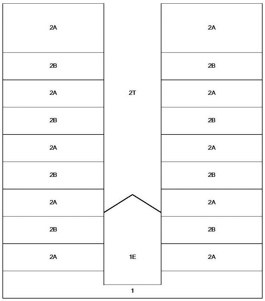
[0024] Such as Figure 3A As shown, a plurality of channel holes are etched and the substrate is epitaxy.

[0025] A substrate 1 is provided, and its material may include bulk silicon (bulkSi), bulk germani...


PUM


Abstract

The invention discloses a production method of a three-dimensional semiconductor device. The method comprises following steps of forming a mask layer stack composed of multiple alternate first and second mask layers on a substrate; etching the mask stack to form channel holes, thus exposing the top of the substrate and the side walls of the first and second mask layers; removing one part of the second mask layers to form hollows; conformally forming blocking layer in the channel holes and the hollows; forming storage layers on the blocking layers; selectively etching so as to remove one part of the storage layers; and conformally forming tunneling layers in the channel holes and the hollows. According to the three-dimensional semiconductor device and the production method of the three-dimensional semiconductor device provided by the invention, the transversely diffused accesses are cut off by utilizing separated storage layer structures; and the data hold characteristic is improved.

Description

technical field [0001] The invention relates to a semiconductor device and a manufacturing method thereof, in particular to a three-dimensional semiconductor storage device and a manufacturing method thereof. Background technique [0002] In order to improve the density of memory devices, the industry has made extensive efforts to develop methods of reducing the size of two-dimensionally arranged memory cells. As the size of memory cells in two-dimensional (2D) memory devices continues to shrink, signal collisions and interference can increase significantly, making it difficult to perform multi-level cell (MLC) operations. In order to overcome the limitations of 2D memory devices, the industry has developed memory devices with a three-dimensional (3D) structure to increase integration density by three-dimensionally arranging memory cells on a substrate. [0003] Specifically, a multi-layer stacked structure (for example, multiple ONO structures alternating with oxides and n...

Claims


Application Information

Patent Timeline
Patent Type & Authority Applications(China)
IPC IPC(8): H01L27/115H01L29/423H01L27/11578
CPCH01L29/42324H10B41/20
Inventor 夏志良霍宗亮
Owner INST OF MICROELECTRONICS CHINESE ACAD OF SCI
Why Eureka
Try Eureka