

led packaging structure and led light emitting device
A technology for LED packaging and light-emitting devices, which is applied to semiconductor devices, electrical components, circuits, etc., can solve the problems of yellow halo of white LED light and poor lighting effect, and achieve the effect of reducing yellow halo.
- Summary
- Abstract
- Description
- Claims
- Application Information
AI Technical Summary
Problems solved by technology
Method used
Image

Examples
Embodiment 1
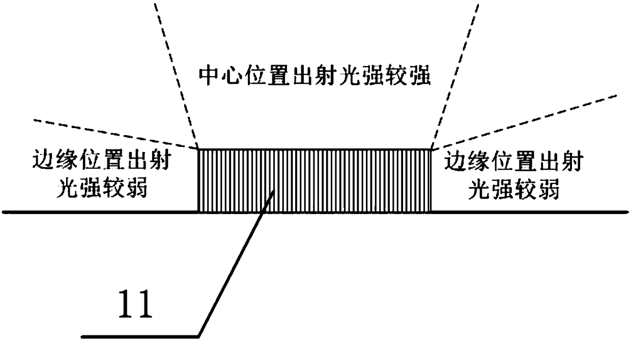
[0050] Figure 4 It is a schematic diagram of an LED packaging structure provided in Embodiment 1 of the present invention. The LED packaging structure in this embodiment can be used in a white LED lighting device, for example, it can be applied to a cool white LED lighting device or a warm white LED lighting device. This embodiment In the example, the color temperature of the LED lighting device is not limited, such as Figure 4 As shown, the LED package structure includes an LED chip 11 and a wavelength conversion material layer 12 .
[0051] Wherein, the wavelength converting substance layer 12 covers the LED chip 11 . Also, the amount of red phosphor in the wavelength conversion material layer 12 is lower at the edge of the LED chip 11 than at the center. Wherein, the wavelength conversion substance layer mentioned here may specifically be a fluorescent adhesive layer containing phosphor powder or other light-transmitting medium layers carrying phosphor powder.
[0052]...
Embodiment 2
[0063] The wavelength conversion material layer 12 mentioned in the first embodiment can be a single-layer structure or a multi-layer structure. In this embodiment, on the basis of the LED package structure provided in the first embodiment, in order to clarify Multi-layer structure, Embodiment 2 provides an example in which the wavelength conversion substance layer 12 is a multi-layer structure.
[0064] Figure 10 One of the schematic diagrams of the LED packaging structure provided for Embodiment 2, such as Figure 10 As shown, the wavelength conversion material layer 12 includes a first sub-wavelength conversion material layer 121 and a second sub-wavelength conversion material layer 122 .
[0065] It should be noted that, for the convenience of description, Figure 10 The LED packaging structure in includes the bowl cup 13, but in actual use, the LED packaging structure may not include the bowl cup 13, therefore, Figure 7 The bowl cup 13 shown in is only used as a kind...
Embodiment 3
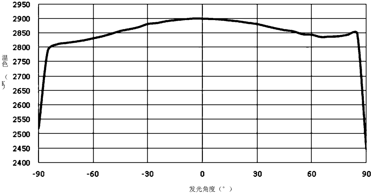
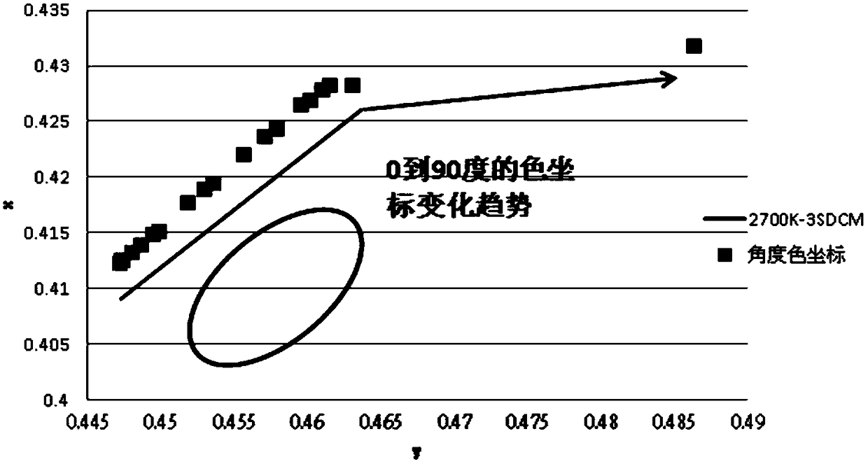
[0082] On the basis of the LED packaging structure provided in Embodiment 1 or Embodiment 2, the distribution of the amount of phosphor powder in the whole is adjusted. In this embodiment, the amount of phosphor powder in the wavelength conversion material layer 12 is higher at the center of the LED chip 11 than at the edge. The amount of phosphor mentioned here refers to the entire amount of phosphor, that is, the total amount of various phosphors.
[0083] It should be noted that the amount of the phosphor here refers to the absolute content of the phosphor, or the mass of the phosphor.
[0084] As a possible implementation, specifically, the thickness of the wavelength conversion material layer 12 remains constant from the center position to the edge position of the LED chip 11, and the wavelength conversion material layer 12 includes yellow and / or green phosphors in the LED chip 11. The concentration of the phosphor powder in the LED chip 11 is higher at the center than a...
PUM
 Abstract
Description
Claims
Application Information