

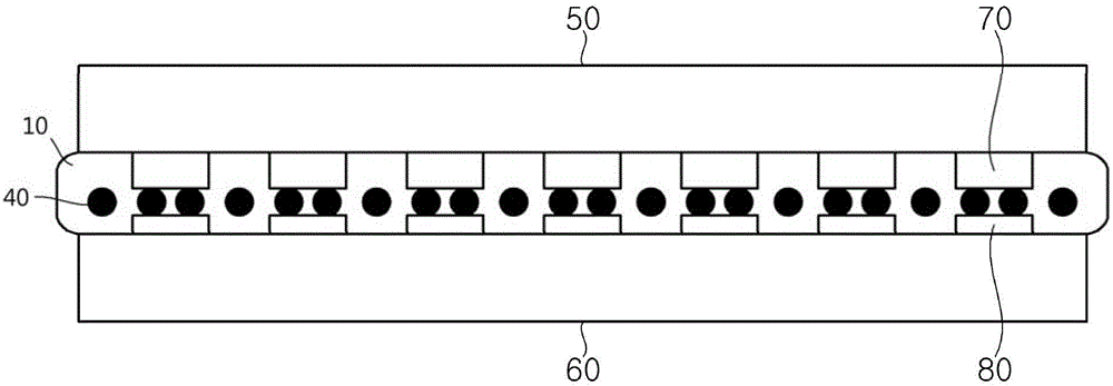
Anisotropic conductive film and semiconductor device using same
An anisotropic, conductive film technology, applied in the direction of semiconductor devices, electric solid devices, conductive layers on insulating carriers, etc., can solve the problems of reducing the flow of the composition, undisclosed adjustment of the anisotropic conductive film of insulating particles, etc. Improve the effect of connection characteristics
- Summary
- Abstract
- Description
- Claims
- Application Information
AI Technical Summary
Problems solved by technology
Method used
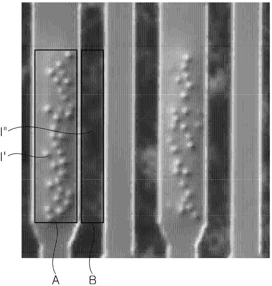
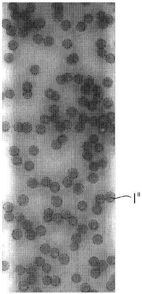
Image

Examples
Embodiment 1
[0136] Preparation of conductive layer composition
[0137] As a binder resin that functions as a matrix for forming a film, 20 parts by weight of a phenoxy resin (PKHH, Inchemrez, USA) dissolved in a xylene / ethyl acetate azeotrope mixed solvent at 40% by volume was used as The curing agent for curing reaction uses 15 parts by weight of propylene oxide epoxy resin (EP-4000S, Adeka, Japan), 10 parts by weight of propylene oxide epoxy resin (EP-4010S, Adeka, Japan), Used as a thermosetting cationic curing agent (Si-60L, Sanshin Chemical, Japan) 5 parts by weight, used as insulating particles for fluidity and insulation (SFP-20M, DENKA, Japan) 30 parts by weight, conductive particles (AUL -704, an average particle size of 4 μm, SEKISUI company, Japan) 20 parts by weight, insulation treatment, and mixing to prepare a conductive layer composition.
[0138] Preparation of insulating layer composition
[0139] When preparing the conductive layer composition, the same method was used to ...
Embodiment 2
[0147] The anisotropic conductive film of Example 2 was produced by the same method and conditions as Example 1, except that the content of each composition was adjusted to be shown in Table 1 in Example 1.
Embodiment 3
[0149] The anisotropic conductive film of Example 3 was produced by the same method and conditions as Example 1, except that the content of each composition was adjusted to be shown in Table 1 in Example 1.
PUM
| Property | Measurement | Unit |
|---|---|---|
| electrical resistance | aaaaa | aaaaa |
| electrical resistance | aaaaa | aaaaa |
| thickness | aaaaa | aaaaa |
Abstract
Description
Claims
Application Information