Polarization-insensitive photic driving tunable TeraHertz wave metamaterial absorber

A polarization-insensitive, light-driven technology used in terahertz applications, which can solve problems such as high absorption fixation

Inactive Publication Date: 2016-06-29
WUHAN UNIV OF SCI & TECH
View PDF1 Cites 35 Cited by
  • Summary
  • Abstract
  • Description
  • Claims
  • Application Information

AI Technical Summary

Problems solved by technology

Although the designed terahertz wave absorber structure can achieve frequency band broadening, the frequency for achieving high absorption is fixed

Method used


Image

  • Polarization-insensitive photic driving tunable TeraHertz wave metamaterial absorber
  • Polarization-insensitive photic driving tunable TeraHertz wave metamaterial absorber
  • Polarization-insensitive photic driving tunable TeraHertz wave metamaterial absorber

Examples


Embodiment 1

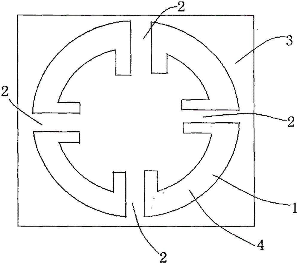
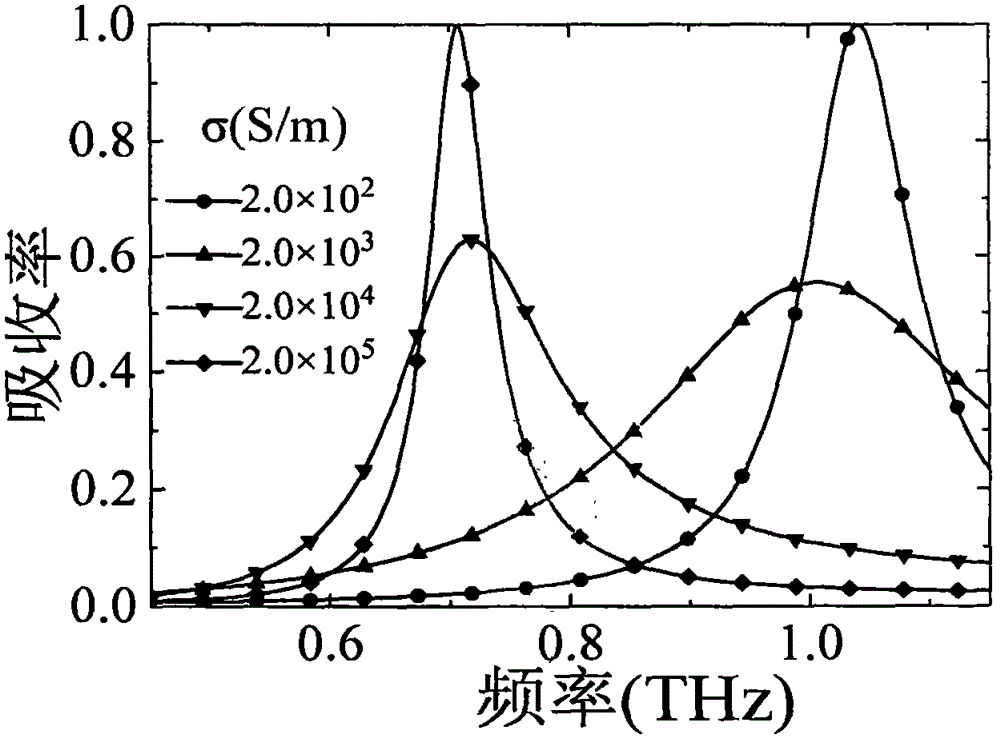
[0035] Example 1, such as figure 1 and figure 2 As shown, the absorber consists of a dielectric substrate 3, a metal pattern layer 4 etched on the dielectric substrate 3 (circular metal slotted ring resonator structure), semiconductor silicon Si embedded in the slotted ring structure, and semiconductor silicon Si conductance The rate σ varies with the light power, and the metal backplane is composed of the figure 1 In the unit structure, the length and width of the first cycle are both p, the outer ring radius of the circular slotted ring is r, the line width is w, the slot width is g, and the metal film thickness of the slotted ring structure is t m , the length of the semiconductor silicon filled at the opening of the slit ring is a. The thickness of the dielectric substrate is t s , the thickness of the metal base plate is t g , by changing the geometric parameters of the unit structure, it can work in different frequency ranges. The variation range of the structural ...

Embodiment 2

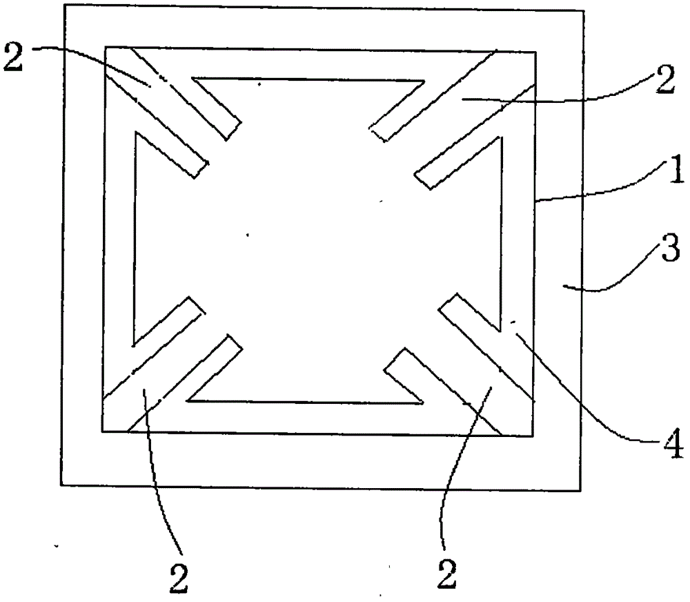
[0049] Example 2, such as image 3 and Figure 4 As shown, the absorber consists of a dielectric substrate 3, a metal pattern layer 4 etched on the dielectric substrate 3 (square metal slotted ring resonator structure), semiconductor silicon Si embedded on the metal pattern layer 4, and the conductivity of the semiconductor silicon Si σ varies with the light power, and is composed of a metal backplane, in which, the length and width of one period of the unit structure are p, the side length of the square is l, the line width is w, the slit width is g, and the metal film thickness of the slotted ring structure is tm, and the length of the semiconductor silicon filled at the opening of the slot ring is a. The thickness of the dielectric base plate is ts, and the thickness of the metal base plate is tg. By changing the geometric parameters of the unit structure, it can work in different frequency ranges. The variation range of the geometric parameters of the basic unit structur...

Embodiment 3

[0061] Embodiment 3, the absorber consists of a dielectric substrate, a metal pattern layer etched on the dielectric substrate (slotted cross-shaped resonator structure), semiconductor silicon Si embedded in the slotted cross, and the conductivity σ of the semiconductor silicon Si increases with The light power varies with the difference, and the metal backplane is composed, in which, the length and width of the unit structure period are p, the side length of the slotted cross is l, the side is w, the slot width is g, and the thickness of the slotted cross-shaped metal film is t m , the length of the semiconductor silicon filled at the cross-shaped opening of the groove is a. The thickness of the dielectric substrate is t s , the thickness of the metal base plate is t g , by changing the geometric parameters of the unit structure, it can work in different frequency ranges. The variation range of the structural geometric parameters of the basic unit of the absorber:

[0062]...


PUM

PropertyMeasurementUnit
thicknessaaaaaaaaaa
widthaaaaaaaaaa
thicknessaaaaaaaaaa

Abstract

The invention provides a polarization-insensitive light-driven tunable terahertz wave metamaterial absorber, which includes a unit structure, a light-sensitive semiconductor, and a metal backplane. The unit structure includes a dielectric substrate, a metal pattern layer, and a metal backplane. The dielectric substrate is located between the metal pattern layer and the metal backplane, the metal pattern layer is embedded with the photosensitive semiconductor, and the unit structure is located on the metal bottom plate. The invention utilizes the difference in conductivity of the loaded semiconductor silicon to adjust the electromagnetic resonance and impedance matching characteristics of the slotted ring structure, so as to realize the adjustment effect of the absorption characteristics in a relatively wide terahertz frequency range. When the terahertz wave is incident on the absorber, a magnetic field loop is generated around the resonant structure. The magnetic field loop causes ohmic loss on the metal sheet and semiconductor silicon, and dielectric loss on the dielectric substrate. The electromagnetic energy of the electromagnetic wave passes through the dielectric loss and The ohmic loss is converted into heat energy, thereby realizing the adjustment of the absorption of the terahertz wave loss.

Description

technical field [0001] The invention belongs to the technical field of terahertz applications of metamaterials and electromagnetic functional materials, and relates to a terahertz absorber, in particular to a polarization-insensitive light-driven tunable terahertz wave metamaterial absorber. Background technique [0002] Terahertz technology is a very important cross-frontier field, which provides a very attractive opportunity for technological innovation, national economic development and national security. Terahertz research involves physics, optoelectronics and material science, etc. It has broad application prospects and application value in the fields of imaging, medical diagnosis, environmental science, information, national security and basic physics research, and has attracted attention from all over the world. Terahertz wave absorbers, which have great application potential in the fields of high-resolution spectral imaging, high data rate short-range communication, ...

Claims


Application Information

Patent Timeline
Patent Type & Authority Applications(China)
IPC IPC(8): H01Q17/00G02B5/00
CPCH01Q17/00G02B5/003
Inventor 程用志章喆周钰杰
Owner WUHAN UNIV OF SCI & TECH
Why Eureka
Try Eureka