Photovoltaic device and preparation deice therefor

A technology of photovoltaic devices and photovoltaic cells, applied in photovoltaic power generation, semiconductor devices, electrical components, etc., can solve problems such as reduced conversion efficiency, leakage, and increase in parallel conductance, so as to increase parallel resistance, increase conversion efficiency, and prevent leakage problems Effect

Active Publication Date: 2016-07-06
SUZHOU INST OF NANO TECH & NANO BIONICS CHINESE ACEDEMY OF SCI
View PDF6 Cites 2 Cited by
  • Summary
  • Abstract
  • Description
  • Claims
  • Application Information

AI Technical Summary

Problems solved by technology

However, due to the significantly smaller resistance of the semi-insulating GaAs substrate under the light, the parallel conductance of the photovoltaic cell increases significantly when the photovoltaic cell is working, that is, the leakage of the PN junction of the photovoltaic cell is serious, resulting in the deformation of the I-V curve, resulting in a decrease in the fill factor and conversion efficiency of the photovoltaic cell.

Method used


Image

  • Photovoltaic device and preparation deice therefor
  • Photovoltaic device and preparation deice therefor
  • Photovoltaic device and preparation deice therefor

Examples


Embodiment 1

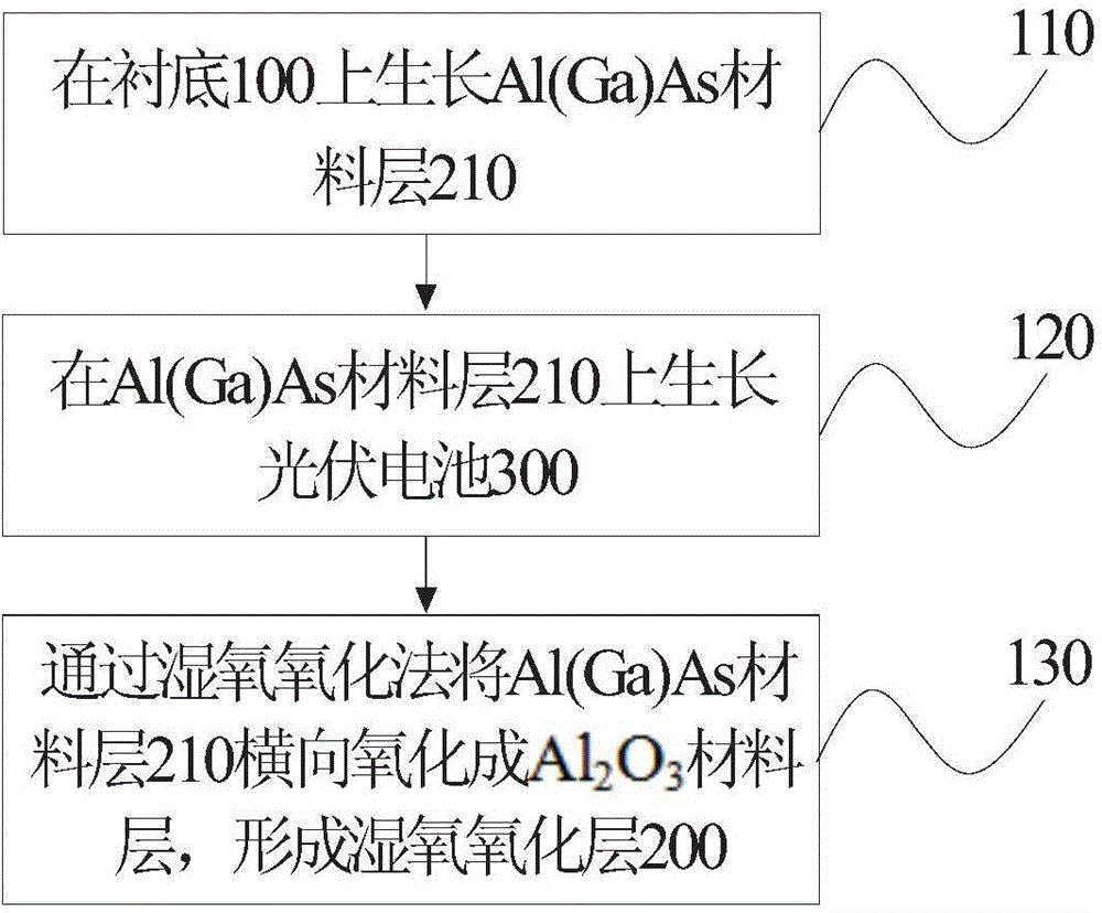
[0030] Steps for growing a single laser photovoltaic cell by metal-organic chemical vapor deposition or molecular beam epitaxy figure 1 ,Specific steps are as follows:

[0031] In step 110 , an Al(Ga)As material layer 210 is grown on the substrate 100 . Specifically, a semi-insulating GaAs substrate 100 is used as a substrate for homogeneous growth of GaAs materials, and its thickness is 200 μm to 500 μm; then the substrate 100 is placed in a growth chamber of metal organic chemical vapor deposition or molecular beam epitaxy, An Al(Ga)As material layer 210 with a thickness of 200nm-500nm is grown on the substrate 100 .

[0032] Wherein, the Al(Ga)As in the Al(Ga)As material layer is Ga 1-x al x As, where x is not less than 0.5.

[0033]In step 120 , a photovoltaic cell 300 is grown on the layer 210 of Al(Ga)As material.

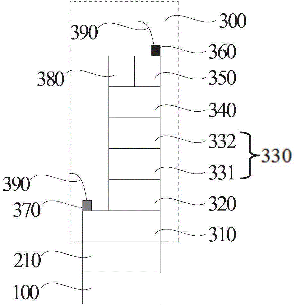
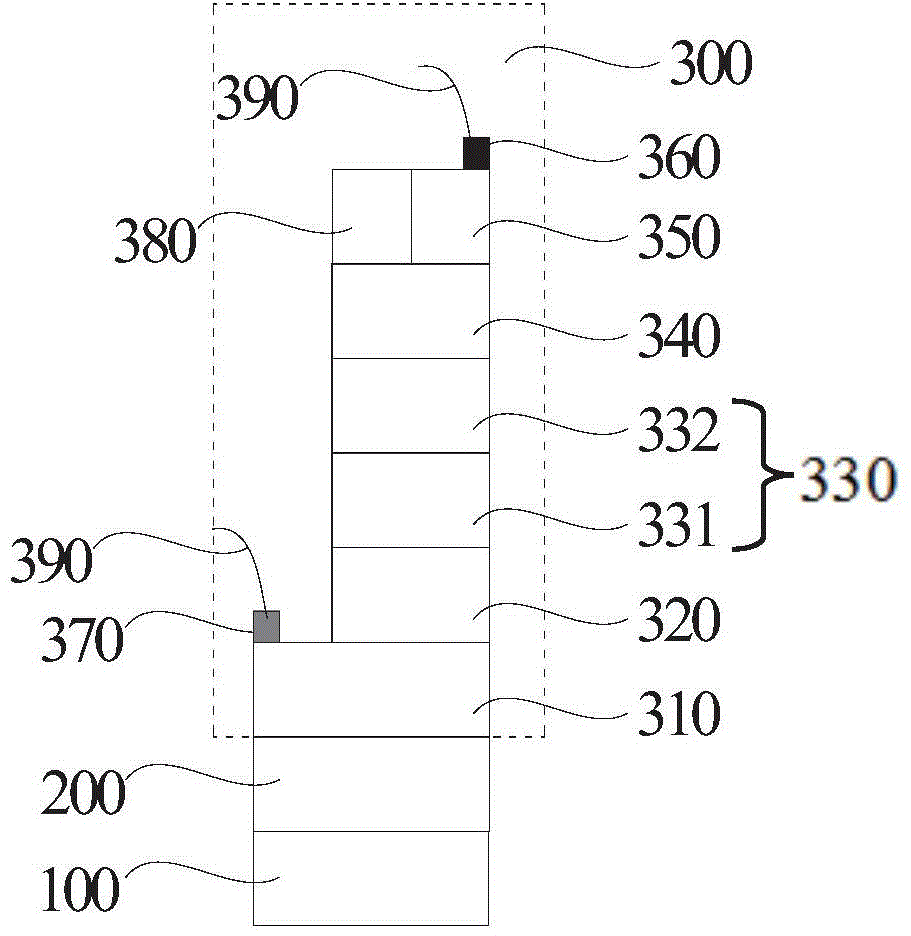
[0034] The specific method is as follows: on the Al(Ga)As material layer 210, N + type contact layer 310, N type back field layer 320, N type base regi...

Embodiment 2

[0045] The laser photovoltaic cell according to the embodiment of the present invention may also be a tandem laser photovoltaic cell, that is, the photovoltaic cell includes several sub-cells connected in series.

[0046] Figure 4 is a flowchart of a method for preparing a tandem laser photovoltaic cell according to an embodiment of the present invention, Figure 5 is a cross-sectional view of a tandem laser photovoltaic cell before wet oxygen oxidation according to an embodiment of the present invention, Image 6 is a cross-sectional view of a tandem laser photovoltaic cell after wet oxygen oxidation according to an embodiment of the present invention.

[0047] The preparation method of the tandem laser photovoltaic cell according to the embodiment of the present invention refers to Figure 4 Specifically, in the description of embodiment 2, the similarity with embodiment 1 is that steps 210, 220, and 240 are respectively similar to steps 110, 120, and 130, and the specifi...


PUM

PropertyMeasurementUnit
thicknessaaaaaaaaaa
thicknessaaaaaaaaaa
thicknessaaaaaaaaaa

Abstract

The invention discloses a photovoltaic device, and the device comprises a substrate and a photovoltaic cell growing on the substrate. The device also comprises an Al2O3 material layer disposed between the substrate and the photovoltaic cell. The invention also discloses a preparation method for the photovoltaic device, and the method comprises the steps: A, growing an Al(Ga)As material layer on the substrate; B, growing the photovoltaic cell on the Al(Ga)As material layer; C, enabling the Al(Ga)As material layer to be laterally oxidized into the Al2O3 material layer through a wet-oxygen oxidation method, and forming a wet-oxygen oxidation layer. The photovoltaic device can effectively prevent a semi-insulating substrate from leaking electricity under solar radiation, also can increase the parallel resistance of the photovoltaic cell, and increases the conversion efficiency.

Description

technical field [0001] The invention relates to the field of photovoltaic devices, in particular to a photovoltaic device and a preparation method thereof. Background technique [0002] The laser energy supply system is an innovative energy transfer system. With this system, the light emitted by the laser source is transmitted to the laser photovoltaic cell through the optical fiber, which can provide a stable power output. The conversion of light into electricity through optical fiber has more advantages than traditional metal wire and coaxial cable power transmission technology, and can be applied in radio communication, industry where electromagnetic interference needs to be eliminated or electronic devices need to be isolated from the surrounding environment. There are important applications in the directions of sensors, national defense, aviation, medicine, and energy. The working principle of laser photovoltaic cells is similar to that of solar cells, except that they...

Claims


Application Information

Patent Timeline
Patent Type & Authority Applications(China)
IPC IPC(8): H01L31/02H01L31/0693H01L31/18
CPCY02E10/544Y02P70/50
Inventor 何洋宋焱董建荣孙玉润赵勇明于淑珍
Owner SUZHOU INST OF NANO TECH & NANO BIONICS CHINESE ACEDEMY OF SCI
Why Eureka
Try Eureka