Method for manufacturing back contact crystalline silicon solar battery piece

A technology for solar cells and a manufacturing method, which is applied in the field of solar cells, can solve the problems of reducing the parallel resistance of cells, increasing the production cost of cells, and reducing the performance of cells, so as to reduce equipment costs, improve parallel resistance and conversion efficiency, The effect of reducing the risk of electric leakage

Active Publication Date: 2015-04-15
盐城阿特斯阳光能源科技有限公司
View PDF3 Cites 0 Cited by
  • Summary
  • Abstract
  • Description
  • Claims
  • Application Information

AI Technical Summary

Problems solved by technology

[0013] In the existing manufacturing process, in the diffusion junction step, a conductive layer that short-circuits the P-N junction will be formed between the backlight surface of the solar cell and the conductive hole, which greatly reduces the parallel resistance of the cell and is prone to leakage, so The conductive layer between the P-N junction needs to be removed by laser isolation step
However, the use of laser isolation may cause new leakage paths in solar cells, resulting in reduced performance of the cells
In addition, the laser damages the cell itself relatively large, and debris may appear during the laser isolation process, which increases the production cost of the cell

Method used


Image

  • Method for manufacturing back contact crystalline silicon solar battery piece
  • Method for manufacturing back contact crystalline silicon solar battery piece
  • Method for manufacturing back contact crystalline silicon solar battery piece

Examples


Embodiment 1

[0059] Please refer to figure 1 , figure 1 The flow chart of the method for manufacturing the back contact crystalline silicon solar cell provided in the first embodiment, as shown in figure 1 As shown, the method includes the following steps:

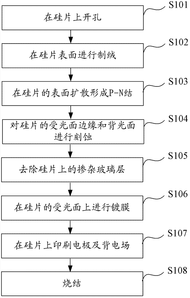
[0060] Step S101: opening holes on the silicon wafer;

[0061] A laser is used to open at least one through hole on the silicon wafer, which can be used to set electrodes in the through hole to lead the current from the light-receiving surface of the battery to the backlight surface of the battery, so that the positive and negative electrodes of the battery can be located on the back of the battery. The back of the sheet reduces the shading rate of the front grid. In the embodiment of the present invention, the wavelength of the laser used for opening holes may be 1064 nm, 1030 nm, 532 nm or 355 nm. The schematic diagram of the structure of the silicon wafer after opening is as follows: figure 2 As shown, 1 in the figure is a sil...

Embodiment 2

[0081] Please refer to Figure 8 , Figure 8 A flow chart of a method for manufacturing a back-contact crystalline silicon solar cell provided in Example 2, as shown in Figure 8 As shown, the method includes the following steps:

[0082] In this embodiment of the present invention, steps 201 to 203 are the same as steps 101 to 103 in Embodiment 1, and will not be repeated here.

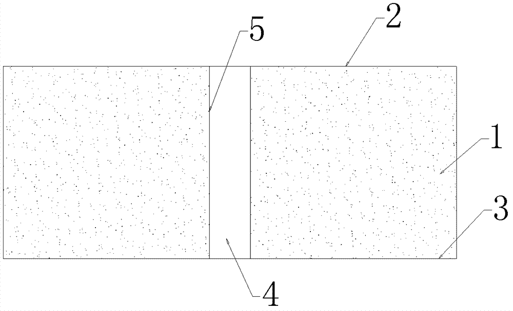
[0083] Step S204: Etching the side surface, backlight surface and all through holes of the silicon wafer;

[0084] Figure 9 It is a schematic diagram of the structure of the silicon wafer after etching, such as Figure 9 As shown, after etching, there is no emitter junction on the inner wall 5 and the side of the through hole. In the embodiment of the present invention, during etching, the entire surface, the entire backlight surface, and all the through holes of the silicon wafer 1 can be completely contacted with the chemical solution, and the contact method can be completely soaked with HF (...

Embodiment 3

[0088] Please refer to Figure 11 , Figure 11 A flow chart of a method for manufacturing a back-contact crystalline silicon solar cell provided in Example 2, as shown in Figure 11 As shown, the method includes the following steps:

[0089] In this embodiment of the present invention, steps 301 to 303 are the same as steps 201 to 203 in Embodiment 2, and will not be repeated here.

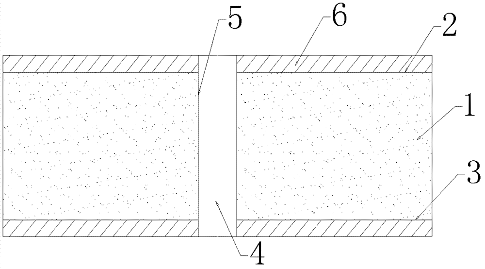
[0090] Step S304: Etching the side surface, the entire backlight surface and some through holes of the silicon wafer;

[0091] Figure 12 It is a schematic diagram of the structure of the silicon wafer after etching, such as Figure 12 As shown, when the through hole is etched, a section of the through hole along the axis of the through hole is selectively etched, so that after etching, there is a local emitter junction on the inner wall 5 of the through hole. In addition, when etching the side surfaces of the silicon wafer, the entire surface of all the sides of the silicon wafer may be etch...


PUM


Abstract

A method for manufacturing a back contact crystalline silicon solar cell sheet is provided. The method comprises: forming a via (4) on a semiconductor wafer (1); performing texturing and diffusion processes on surfaces (2, 3) of the semiconductor wafer; etching the diffused semiconductor wafer and performing the subsequent processes, thus obtaining the back contact crystalline silicon solar cell sheet, wherein the etching includes etching the backlight surface (3) and the edge of the light receiving surface (2) of the semiconductor wafer. In the method, the edge of the light receiving surface of the wafer and the emitter junction formed by diffusing on the backlight surface of the wafer are removed by etching at the same time. So there is not a short circuit conductive layer between the backlight surface and the conductive via of the solar cell sheet. Compared with the prior art, the method avoids the laser isolating process and then reduces the risk of leakage and the breakage rate of the cell sheet.

Description

technical field [0001] The invention relates to the technical field of solar cells, in particular to a method for manufacturing back-contact crystalline silicon solar cells. Background technique [0002] A solar cell, also known as a photovoltaic cell, is a semiconductor device that converts the sun's light energy directly into electrical energy. Because it is a green product, does not cause environmental pollution, and is a renewable resource, solar cells are a new energy source with broad development prospects in today's energy shortage situation. At present, more than 80% of solar cells are made of crystalline silicon materials. Therefore, the preparation of high-efficiency crystalline silicon solar cells is of great significance for large-scale utilization of solar power generation. The main grid line, the positive electrode and the negative electrode are all located on the backlight side of the cell, which greatly reduces the shading rate of the light-receiving surface...

Claims


Application Information

Patent Timeline
Patent Type & Authority Patents(China)
IPC IPC(8): H01L31/18
CPCH01L31/1804H01L31/02245H01L31/068Y02E10/547Y02P70/50
Inventor 章灵军张凤吴坚王栩生
Owner 盐城阿特斯阳光能源科技有限公司
Why Eureka
Try Eureka