Deposition assembly and semiconductor processing equipment

A technology for deposition components and deposition rings, which is applied in semiconductor/solid-state device manufacturing, electrical components, metal material coating technology, etc., can solve problems such as adverse effects of cooling wafer uniformity, wafer 14 deviation, and high processing difficulty, so as to avoid Adverse effects, improvement of process efficiency, and effect of reducing processing difficulty

Active Publication Date: 2016-07-20
BEIJING NAURA MICROELECTRONICS EQUIP CO LTD
View PDF5 Cites 5 Cited by
  • Summary
  • Abstract
  • Description
  • Claims
  • Application Information

AI Technical Summary

Problems solved by technology

[0006] One, because the above-mentioned thimble 13 can only support the wafer 14, but cannot limit the position of the wafer 14 in its radial direction, this makes the wafer 14 often shift due to the movement of the thimble 13 or the interference of the vibration of the surrounding equipment, so that when After the base 10 rises and lifts up the wafer 14 on the

Method used


Image

  • Deposition assembly and semiconductor processing equipment
  • Deposition assembly and semiconductor processing equipment
  • Deposition assembly and semiconductor processing equipment

Examples


Embodiment Construction

[0043] In order for those skilled in the art to better understand the technical solution of the present invention, the deposition assembly and semiconductor processing equipment provided by the present invention will be described in detail below with reference to the accompanying drawings.

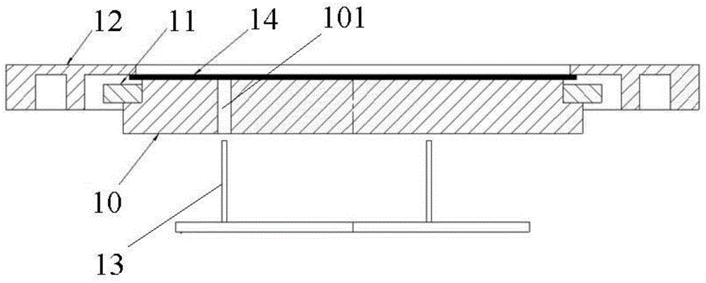
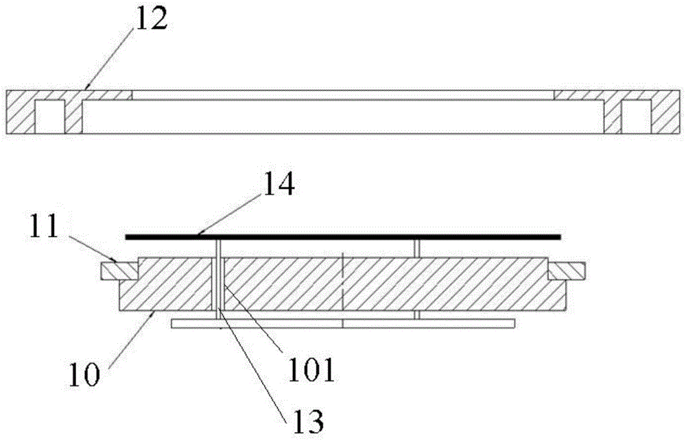
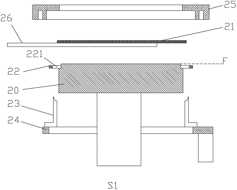
[0044] Please also refer to Figure 2A-Figure 2D , the deposition assembly is used to transfer and fix the wafer 21 on the base 20, the base 20 is liftable, and it can rise to such as Figure 2A process position E as shown, or down to as Figure 2B Loading and unloading position F shown. The so-called process position refers to the highest position where the pre-set base is raised to process the wafer. The so-called loading and unloading position refers to the lowest position where the base is lowered to the preset position for taking / putting the film from the base.

[0045] The deposition assembly includes a deposition ring 22 , a snap ring 25 and four thimbles 23 . Among them, the de...


PUM


Abstract

The invention provides a deposition assembly and semiconductor processing equipment which are used for transferring wafers and fixing the wafers to a base. The base is lifted to a technology position or descended to a loading and unloading position by going up and down. The deposition assembly comprises a deposition ring, a clamping ring and at least three thimbles, wherein the thimbles are distributed in the circumferential direction of the base; in addition, when the base is located in the loading and unloading position, the thimbles penetrate through the deposition ring by going up and down, so that the plane where the top ends of the thimbles is higher or lower than the upper surface of the base. Moreover, a positioning convex part is arranged on the bearing surface of each thimble, and the bearing surfaces are used for supporting the wafers. The positioning convex parts are used for preventing the wafers from moving in the radial direction of the wafers when the wafers are supported by the thimbles. According to the deposition assembly provided by the invention, not only can the radial positions of the wafers on the thimbles be limited by the deposition assembly, but also the processing difficulty of the base can be reduced; and in addition, the harmful effect on the uniformity of the base cooling wafers due to the fact that a through hole is machined in the base is avoided.

Description

technical field [0001] The invention belongs to the technical field of semiconductor equipment manufacturing, and in particular relates to a deposition component and plasma processing equipment. Background technique [0002] In the manufacturing fields of integrated circuits, liquid crystal displays, thin-film solar energy, and LEDs, physical vapor deposition (Physical Vapor Deposition, hereinafter referred to as PVD) technology is usually used to deposit materials such as metal layers on wafers. During the process, it is usually necessary to set a carrier device (such as an electrostatic chuck or a mechanical chuck) in the reaction chamber to carry the wafer, and use the thimble device to transfer the wafer to the electrostatic chuck or mechanical chuck, and then the The ring holds the wafer. [0003] Figure 1A A cross-sectional view of an existing deposition assembly in process position. Figure 1B It is a cross-sectional view of the existing deposition assembly when it...

Claims


Application Information

Patent Timeline
IPC IPC(8): C23C14/50H01L21/683
Inventor 郭浩侯珏郑金果杨敬山赵梦欣陈鹏
Owner BEIJING NAURA MICROELECTRONICS EQUIP CO LTD
Why Eureka
Try Eureka