Method for improving profile of side wall of grid electrode, and semiconductor device manufacturing method

A gate sidewall and semiconductor technology, which is applied in the manufacture of semiconductor/solid-state devices, electrical components, circuits, etc., can solve problems such as inability to insulate the gate from the contact hole 13, deterioration of device performance, and affect the quality of the device, so as to achieve an improvement threshold Voltage and leakage current issues, improving device performance, and reducing etching loss

Active Publication Date: 2016-07-20
SHANGHAI HUAHONG GRACE SEMICON MFG CORP
View PDF5 Cites 7 Cited by
  • Summary
  • Abstract
  • Description
  • Claims
  • Application Information

AI Technical Summary

Problems solved by technology

The sloping shoulder at the top of the existing side wall structure 12 is relatively sharp, which is likely to cause some defects:
[0004] 1. When a large dose of source / drain region implantation 14 is performed on the semiconductor substrate 10 with the sidewall structure 12 as a mask, the implanted ions will easily pass through the sidewall structure 12 and penetrate into the gate, resulting in a threshold voltage Vt of the device and leakage current increase significantly, seriously affecting the quality of the device;
[0005] 2. When the contact hole (CT) 13 is made on the source / drain region of the semiconductor substrate 10, it is easy to generate a stack shift (overlayshift). If both the minimum horizontal distance D1 and the maximum horizontal distance D2 between the gates are reduced, the spacer structure 12 can no longer completely insulate the gate and the contact hole 13, and it is very likely to cause a gap between the gate and the contact hole 13. leakage phenomenon, and eventually degrade the performance of the device

Method used


Image

  • Method for improving profile of side wall of grid electrode, and semiconductor device manufacturing method
  • Method for improving profile of side wall of grid electrode, and semiconductor device manufacturing method
  • Method for improving profile of side wall of grid electrode, and semiconductor device manufacturing method

Examples


Embodiment Construction

[0031] In order to make the purpose and features of the present invention more comprehensible, the specific embodiments of the present invention will be further described below with reference to the accompanying drawings. However, the present invention can be implemented in different forms and should not be limited to the described embodiments.

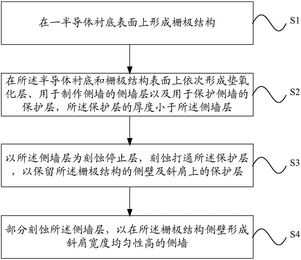
[0032] Please refer to figure 2 , This embodiment provides a method for improving the topography of the sidewall of the gate, including:

[0033] S1, forming a gate structure on the surface of a semiconductor substrate;

[0034] S2, forming a pad oxide layer, a sidewall layer for making sidewalls, and a protective layer for protecting the sidewalls in sequence on the surface of the semiconductor substrate and the gate structure, the thickness of the protection layer is smaller than that of the sidewalls Floor;

[0035] S3, using the sidewall layer as an etch stop layer, and etch through the protective layer to retain the protective layer on ...


PUM


Abstract

The invention provides a method for improving the profile of a side wall of a grid electrode, and a semiconductor device manufacturing method. The method for improving the profile of the side wall of the grid electrode comprises the steps: covering the surface of a formed side wall layer with a protection layer, wherein the protection layer covers the side wall layer, thereby enabling the surface of a semiconductor substrate to tend to be flat; carrying out the vertical etching of the protection layer through employing the punchthrough etching technology with the high etching selection ratio of the side wall layer and the protection layer, so as to remove a part, located on a top plane of a grid structure, of the protection layer, and keep the parts located on side walls and an inclined shoulder of the grid structure; enabling the protection layer on the inclined shoulder to be able to protect the side wall layer below the protection layer in a process of forming the side wall through the partial etching of the side wall layer, thereby reducing the etching loss of a side wall material on the inclined shoulder, and finally obtaining the side wall with the width uniformity. The side wall can increase the effective distance between a contact hole, sequentially formed in a source / drain region, and the grid structure, improves the effect of ion injection of the source / drain regions, solves problems of threshold voltage and leaked current of a device, and improves the performance of the device.

Description

Technical field [0001] The invention relates to the field of semiconductor manufacturing, in particular to a method for improving the shape of a gate sidewall and a method for manufacturing a semiconductor device. Background technique [0002] Please refer to figure 1 After the semiconductor manufacturing process enters the nanometer level, spacers 12 are generally used in CMOS devices. The spacers 12 surround the gate 11, which can protect the polysilicon gate and define the source and drain ion implantation of the semiconductor substrate 10. To prevent bridging caused by self-aligned silicide, and to prevent high-intensity and large-dose source / drain implantation 14 from being too close to the channel to cause source / drain punchthrough. [0003] The method of forming the sidewall structure 12 in the prior art usually includes, after the gate 11 is formed, a layer of sidewall material is deposited on the surface of the gate 11 and the semiconductor substrate, and then the semicond...

Claims


Application Information

Patent Timeline
Patent Type & Authority Applications(China)
IPC IPC(8): H01L21/8234H01L21/8238
Inventor 陈宏
Owner SHANGHAI HUAHONG GRACE SEMICON MFG CORP
Why Eureka
Try Eureka