Stacked filter and image sensor containing the same

An image sensor and optical filter technology, which is applied in the field of stacked optical filters, can solve the problems of optical filter offset, etc., and achieve the effect of easy manufacturing and avoiding the phenomenon of blue shift

Inactive Publication Date: 2016-07-20
VISERA TECH CO LTD
View PDF12 Cites 16 Cited by
  • Summary
  • Abstract
  • Description
  • Claims
  • Application Information

AI Technical Summary

Problems solved by technology

However, traditional optical filters are usually manufactured by multi-layer film interference technology. When the incident light with a large oblique angle falls on the traditional opti...

Method used


Image

  • Stacked filter and image sensor containing the same
  • Stacked filter and image sensor containing the same
  • Stacked filter and image sensor containing the same

Examples


Embodiment Construction

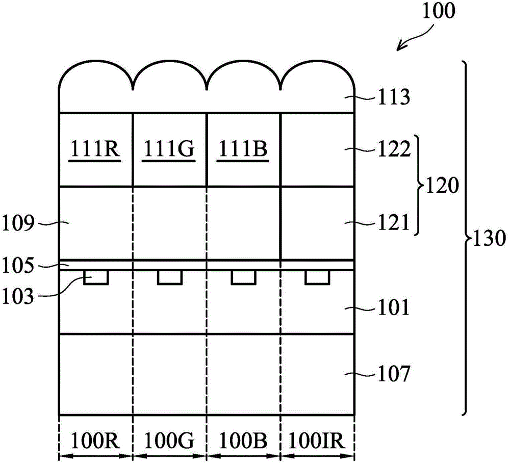
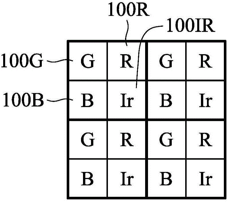
[0048] Refer to figure 1 , Which shows a schematic cross-sectional view of a part of a backside illumination (BSI) image sensor 100 according to some embodiments disclosed in the present invention. The image sensor 100 has a plurality of red pixels 100R, green pixels 100G, blue pixels 100B and infrared pixels 100IR arranged in a pixel array in sequence. figure 2 In accordance with some embodiments disclosed in the present invention, the red pixel 100R, the green pixel 100G, the blue pixel 100B, and the infrared pixel 100IR of the image sensor 100 are arranged in a schematic plan view. Such as figure 2 As shown, in the Bayer pattern in which the red pixel 100R, the green pixel 100G, the blue pixel 100B, and the infrared pixel 100IR are arranged, an original green pixel is replaced by an infrared pixel.

[0049] Such as figure 1 As shown, the image sensor 100 includes a semiconductor substrate 101, and the semiconductor substrate 101 includes a plurality of photodiodes 103 formed ...


PUM

PropertyMeasurementUnit
Wavelengthaaaaaaaaaa

Abstract

The invention discloses a stacked filter for an image sensor containing an infrared ray pixel. The stacked filter includes a first filter layer disposed at the IR pixel. The first filter layer allows light with wavelengths of a first band to be transmitted through. The stacked filter further includes a second filter layer stacked with the first filter layer. The second filter layer allows light with wavelengths of a second band to be transmitted through. The first band partially overlaps the second band at wavelengths of a third band. The third band is narrower than the first band and the second band. The stacked filter allows light with the wavelengths of the third band to be transmitted through. Furthermore, an image sensor containing a stacked filter is also provided. The stacked filter is easy to manufacture, and the characteristics of the stacked filter have no relation with the angle of the incident ray and are not influenced by the angle of the incident ray. Therefore, the stacked filter can avoide generation of blue shift situation when an inclined incident ray with a large angle irradiates on the image sensor.

Description

Technical field [0001] The present invention relates to the field of stacked filters, in particular to a stack of image sensors that integrates infrared pixels and red, green and blue pixels in a single sensor in the application of time-of-flight (ToF) technology Filters and image sensors with stacked filters. Background technique [0002] At present, time-of-flight (ToF) technology has been widely used in modern industries, and can provide three-dimensional (3D) images through the combination of complementary metal oxide semiconductor (CMOS) pixel arrays and adjustable light sources . Three-dimensional time difference (3DToF) cameras have been used in many different applications, such as contour inspection of manufactured goods, computer aided design (CAD) verification, geographic measurement, and object imaging. [0003] The operation of the three-dimensional time difference ranging (3DToF) camera is to use an adjustable light source to illuminate the scene, observe the light r...

Claims


Application Information

Patent Timeline
IPC IPC(8): H01L27/146
CPCG02B5/201H01L27/14621H01L27/14649H01L27/14645H01L27/1464G02B5/22H01L27/14627H01L27/14685H01L27/14652
Inventor 王唯科
Owner VISERA TECH CO LTD
Why Eureka
Try Eureka