Method for manufacturing an organic light-emitting display panel

A technology of light-emitting display and manufacturing method, which is applied in the direction of static indicators, semiconductor/solid-state device manufacturing, instruments, etc., and can solve the problems that light-emitting devices do not contribute to light emission, affect the display effect of display devices, and affect the working performance of electronic components.

Active Publication Date: 2018-06-22
BOE TECH GRP CO LTD
View PDF8 Cites 0 Cited by
  • Summary
  • Abstract
  • Description
  • Claims
  • Application Information

AI Technical Summary

Problems solved by technology

However, compared with the blue light pixel, the excessively shared voltage and corresponding power consumption of the driving transistors in the active driving circuit of the red and green pixels do not contribute to the light emission of the light-emitting device, but become heat dissipation, which not only reduces the display device Electro-optical efficiency, and because the heat in the circuit reaches a certain level, it will affect the performance of electronic components, thus affecting the display effect of the display device

Method used


Image

  • Method for manufacturing an organic light-emitting display panel
  • Method for manufacturing an organic light-emitting display panel
  • Method for manufacturing an organic light-emitting display panel

Examples


Embodiment Construction

[0033] An embodiment of the present invention provides a method for manufacturing an organic light-emitting display panel, which is used to reduce the voltage drop generated by the wiring resistance of the pixel active driving circuit in the pixel structure, reduce the energy loss caused by thermal power consumption, and improve the electro-optical efficiency of the display device .

[0034] The technical solutions provided by the embodiments of the present invention are specifically described below with reference to the accompanying drawings.

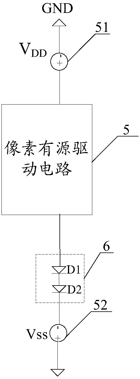
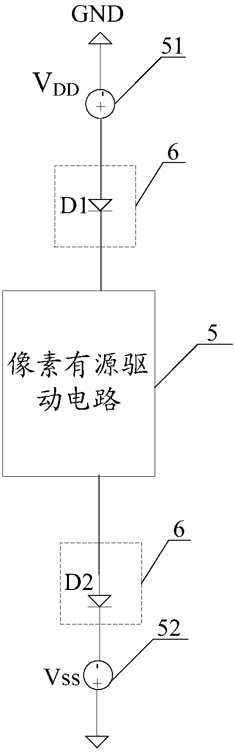
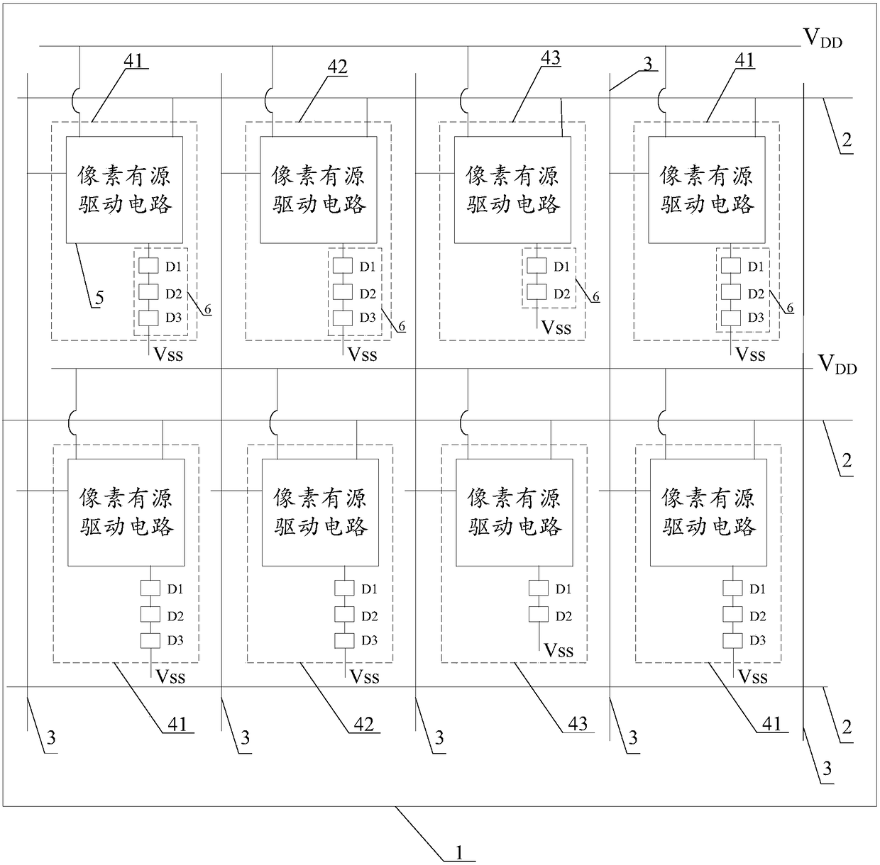
[0035] see figure 1 , the pixel structure provided by the embodiment of the present invention includes:

[0036] Pixel active drive circuit 5;

[0037] A light-emitting device group 6 connected to the pixel active drive circuit 5; the light-emitting device group 6 includes at least two light-emitting devices connected in series, such as figure 1 The light emitting device D1 and the light emitting device D2 in.

[0038] The pixel ac...


PUM


Abstract

An embodiment of the present invention provides a method for manufacturing an organic light-emitting display panel, which is used to improve the electro-optical efficiency of a display device. The method includes: forming a first anode and a second anode on a substrate, sequentially forming a first hole transport layer, a first organic light-emitting layer, a first electron transport layer, a An insulating layer and a first cathode in a certain width area on the side of the organic light-emitting layer; a second hole transport layer, a second organic light-emitting layer, and a second electron transport layer are sequentially formed on the second anode, and are located on the periphery of the second anode The insulating layer, the second cathode; the second cathode is partly connected to the first anode.

Description

[0001] The present invention application is a divisional application of an invention application with a filing date of December 13, 2012, an application number of 201210539995.X, and an invention title of "a pixel structure, a pixel unit structure, a display panel, and a display device". technical field [0002] The present invention relates to the field of organic light emitting technology, in particular to a method for manufacturing an organic light emitting display panel. Background technique [0003] Organic light-emitting displays are called the next generation of fantasy because of their advantages such as full solid state, active light emission, high contrast, ultra-thin, low power consumption, wide viewing angle, fast response, wide working range, and easy realization of flexible display and 3D display. monitor. At the same time, since the light-emitting device has the feature of being able to form a large-area film, it can become an ideal large-size flat panel displ...

Claims


Application Information

Patent Timeline
Patent Type & Authority Patents(China)
IPC IPC(8): H01L51/56
CPCH10K71/441H10K59/1315G09G3/3225G09G2300/0452G09G2300/08G09G2330/021H10K59/86G09G3/30G09G3/32G09G3/3233H10K59/353H10K59/12
Inventor 皇甫鲁江马占洁
Owner BOE TECH GRP CO LTD
Why Eureka
Try Eureka