

MEMS (Micro Electro Mechanical Systems) cantilever structure and manufacturing method thereof
A technology of cantilever beam and dry etching, which is applied in the field of semiconductors, can solve the problems of adhesion to base materials, fracture free moving ends, adhesion, etc., and achieve the effects of reducing contact area, reducing fracture risk, and preventing adhesion
- Summary
- Abstract
- Description
- Claims
- Application Information
AI Technical Summary
Problems solved by technology
Method used
Image

Examples
Embodiment Construction
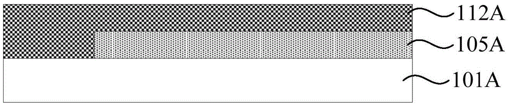
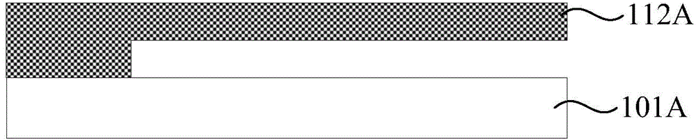
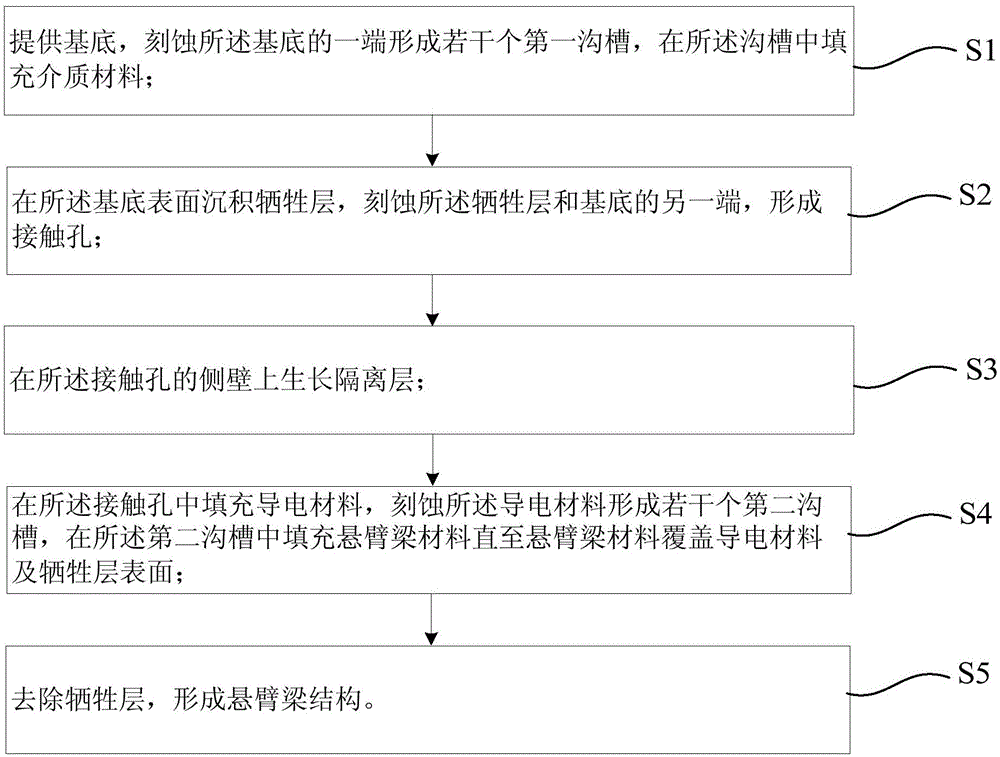
[0050] Embodiments of the present invention are described below through specific examples, and those skilled in the art can easily understand other advantages and effects of the present invention from the content disclosed in this specification. The present invention can also be implemented or applied through other different specific implementation modes, and various modifications or changes can be made to the details in this specification based on different viewpoints and applications without departing from the spirit of the present invention.
[0051] Please refer to attached picture. It should be noted that the diagrams provided in this embodiment are only schematically illustrating the basic idea of the present invention, and only the components related to the present invention are shown in the diagrams rather than the number, shape and shape of the components in actual implementation. Dimensional drawing, the type, quantity and proportion of each component can be change...
PUM
| Property | Measurement | Unit |
|---|---|---|
| depth | aaaaa | aaaaa |
Abstract
Description
Claims
Application Information