Method for eliminating shallow trench isolation induced dark current of CMOS image sensor

An image sensor and shallow groove technology, applied in the direction of circuits, electrical components, electric solid devices, etc., can solve problems such as surface damage, easy release of electrons, and increased surface area of ​​grooves, so as to avoid dark current, reduce dark current, Effect of suppressing dark current increase

Inactive Publication Date: 2016-08-17
SHANGHAI HUALI MICROELECTRONICS CORP
View PDF3 Cites 3 Cited by
  • Summary
  • Abstract
  • Description
  • Claims
  • Application Information

AI Technical Summary

Problems solved by technology

Deeper STI trenches result in increased trench surface area
The surface of the STI groove will be damaged by the etching process, subsequent high-density plasma chemical vapor deposition and other processes, that is, the SI-bond on the silicon surface is interrupted by plasma and other processes, and the dangling silicon bond is easy to capture electrons. But it is also easy to release trapped electrons

Method used


Image

  • Method for eliminating shallow trench isolation induced dark current of CMOS image sensor
  • Method for eliminating shallow trench isolation induced dark current of CMOS image sensor

Examples


Embodiment Construction

[0023] In order to make the content of the present invention clearer and easier to understand, the content of the present invention will be described in detail below in conjunction with specific embodiments and accompanying drawings.

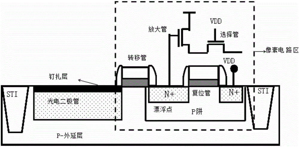
[0024] Before explaining the principle of the present invention in detail, the original two active region cycle process steps are briefly described. Specifically, the original two active region cycle process steps are as follows:

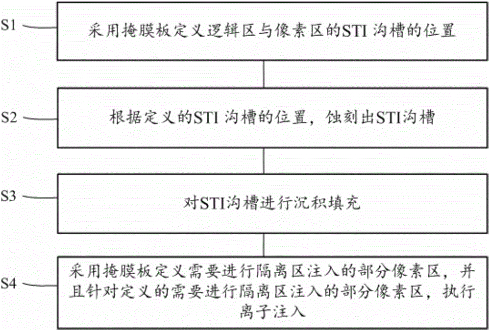
[0025] Firstly, a mask plate is used to define the position of the thicker STI groove (herein referred to as the first STI groove);

[0026] Subsequently, etching an initial first depth of the first STI trench;

[0027] Thereafter, the positions of all STI grooves are defined by using a mask;

[0028] Thereafter, etching is performed on all the STI trenches, wherein the second STI trench except the first STI trench among all the STI trenches has a second depth, and the depth of the first STI trench is equal to the f...


PUM


Abstract

The invention provides a method for eliminating shallow trench isolation induced dark current of a CMOS image sensor. The method comprises the step of step 1: defining positions of STI trenches of a logic region and a pixel region through mask plates; step 2: etching the STI trenches according to the defined positions of the STI trenches; step 3: carrying out disposition and filling on the STI trenches; and step 4: defining a part of pixel regions which need to be subjected to isolation region injection by adopting the mask plates, and carrying out ion implantation for the part of the defined pixel regions which need to be subjected to isolation region injection.

Description

technical field [0001] The invention relates to the field of semiconductor manufacturing, more specifically, the invention relates to a method for eliminating dark current induced by shallow trench isolation of a CMOS image sensor. Background technique [0002] CMOS image sensor (CIS) is compatible with the existing integrated circuit manufacturing process because of its manufacturing process, and has many advantages in performance compared with the original charge-coupled device CCD. The CMOS image sensor can integrate the driving circuit and the pixel together, which simplifies the hardware design and reduces the power consumption of the system at the same time. Because CIS can take out electrical signals while collecting optical signals, it can also process image information in real time, and its speed is faster than that of CCD image sensors. CMOS image sensors also have the advantages of low price, large bandwidth, anti-blur, flexible access and large fill factor. [...

Claims


Application Information

Patent Timeline
Patent Type & Authority Applications(China)
IPC IPC(8): H01L21/266H01L21/762H01L27/146
CPCH01L27/14689H01L21/266H01L21/76224
Inventor 白英英李娟娟田志陈昊瑜
Owner SHANGHAI HUALI MICROELECTRONICS CORP
Why Eureka
Try Eureka