Preparation method of transparent conductive oxide film
An oxide film, transparent and conductive technology, applied in the field of solar cells, can solve the problems of affecting the conversion efficiency of solar cells, increasing the cost of film preparation, and poor film compactness, so as to improve the open circuit voltage and filling effect, mobility and light transmittance Effect of improvement, conversion efficiency improvement
- Summary
- Abstract
- Description
- Claims
- Application Information
AI Technical Summary
Problems solved by technology
Method used
Image
Examples
preparation example Construction
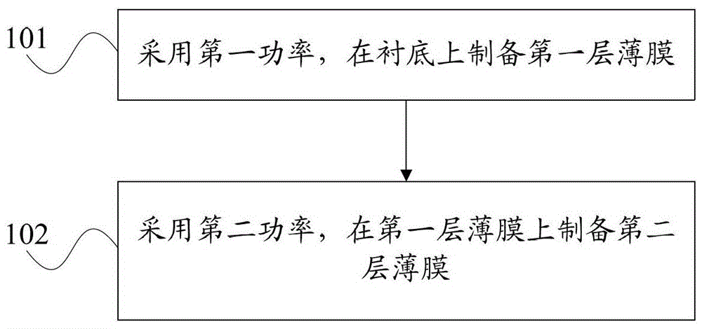
[0026] Based on this, the present invention provides a method for preparing a transparent conductive oxide film, which is applied to magnetron sputtering equipment to overcome the above-mentioned problems in the prior art, including: using the first power to prepare the first A thin film; using a second power to prepare a second thin film on the first thin film; wherein, the second power is greater than the first power.
[0027] The preparation method of the transparent conductive oxide film provided by the present invention first adopts low power to prepare a layer of TCO film. During this process, the energy of the sputtered particles is low, and the damage to the substrate is small, and the prepared film is smooth and dense. Uniform, and a good interface is formed between the TCO film prepared by low power and the substrate, which reduces the defect density of the interface, improves the open circuit voltage and filling effect, and the TCO film prepared by low power plays a ...
Embodiment 1
[0033] The flow chart of the preparation method of the transparent conductive oxide film disclosed in this embodiment is as follows figure 1 As shown, it is applied to magnetron sputtering equipment, and the specific steps are as follows:
[0034] Step 101: Using the first power, prepare a first film on the substrate.
[0035] Wherein, the first power is 1W-500W, inclusive, the thickness of the first thin film is 3nm-20nm, inclusive, and the substrate is a solar battery sheet before TCO film preparation. When the TCO film is prepared with a lower first power, the energy of the sputtered particles is lower, and the damage to the substrate is less, and in this process, the deposition rate of the TCO film is low, about 0.2nm / s~2nm / s, including the endpoint value, therefore, the prepared TCO film has uniform deposition, dense arrangement and smooth surface, and at the same time, a good interface is formed between the TCO film and the substrate, which reduces the defect density o...
Embodiment 2
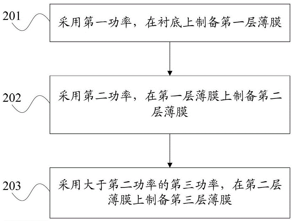
[0043] The flow chart of the preparation method of the transparent conductive oxide thin film disclosed in this embodiment is as follows figure 2 As shown, it is applied to magnetron sputtering equipment, and the specific steps are as follows:
[0044] Step 201: Using the first power, prepare a first film on the substrate.
[0045] Wherein, the first power is 1W-500W, inclusive, the thickness of the first thin film is 3nm-20nm, inclusive, and the substrate is a solar battery sheet before TCO film preparation. When the TCO film is prepared with a lower first power, the energy of the sputtered particles is lower, and the damage to the substrate is less, and in this process, the deposition rate of the TCO film is low, about 0.2nm / s~2nm / s, including the endpoint value, therefore, the prepared TCO film has uniform deposition, dense arrangement and smooth surface, and at the same time, a good interface is formed between the TCO film and the substrate, which reduces the defect den...
PUM
| Property | Measurement | Unit |
|---|---|---|
| thickness | aaaaa | aaaaa |
| thickness | aaaaa | aaaaa |
Abstract
Description
Claims
Application Information


