Preparation method and system of TOPCon solar cell silicon oxide layer

A technology for solar cells and silicon oxide layers, applied in circuits, photovoltaic power generation, electrical components, etc., can solve the problems of slow oxide layer film formation, bombardment damage to silicon wafer substrates, and slag removal, so as to avoid bombardment damage and equipment maintenance. High frequency, solve the effect of slow film formation

Pending Publication Date: 2021-01-26
江苏杰太光电技术有限公司
View PDF0 Cites 2 Cited by
  • Summary
  • Abstract
  • Description
  • Claims
  • Application Information

AI Technical Summary

Problems solved by technology

[0005] 1. The thermal oxidation method is to place the silicon wafer in a clean quartz tube, and heat the tube furnace through a resistance wire to reach a reaction temperature of about 600°C, so that the silicon wafer and the incoming O 2 The process of chemical reaction to form an oxide layer; the oxidation process generally takes about 30-60 minutes to grow an oxide layer, and it takes more than 10 minutes for the silicon wafer to enter and exit the quartz tube. , low production capacity; in addition, the resistance wire is used to heat the tube furnace first, and the heat is transmitted from the outer wall of the furnace tube to the inner wall of the furnace and the silicon wafer in turn. This indirect heating has slow heating speed and high energy consumption;
[0006] 2. Using PECVD technology to deposit silicon oxide film, using O 2 or O 2 The mixed gas of nitrous oxide and silane is used as the process gas to generate highly active N / O ions under the action of the plasma, which chemically reacts with the silicon wafer to form a silicon oxide film on its surface; however, the use of plasma will cause silicon wafer A certain degree of bombardment damage to the substrate leads to a decrease in efficiency, and the reactants are also easy to deposit inside the cavity. Long-term accumulation is prone to the problem of slag falling, which will affect the production yield and bring relatively big problems to equipment maintenance.

Method used


Image

  • Preparation method and system of TOPCon solar cell silicon oxide layer
  • Preparation method and system of TOPCon solar cell silicon oxide layer

Examples


Embodiment Construction

[0023] The following will clearly and completely describe the technical solutions in the embodiments of the present invention with reference to the drawings in the embodiments of the present invention.

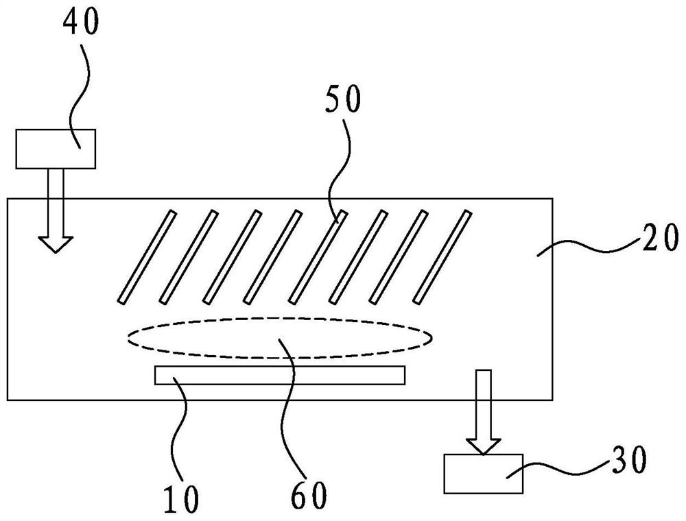
[0024] refer to figure 1 The preparation system of shown TOPCon solar cell silicon oxide layer, the invention provides a kind of preparation method of TOPCon solar cell silicon oxide layer, comprises the steps:

[0025] S1. First place the silicon wafer flat on the carrier plate 10 and transport the carrier plate 10 into the process chamber 20 through the horizontal conveying line; wherein, the carrier plate 10 with the silicon wafer placed on it passes through the process chamber 20 continuously to realize the dynamic growth of silicon oxide film , or pause in the process chamber 20 to achieve static growth of the silicon oxide film;

[0026] S2. After the silicon wafer enters the process chamber 20, the process chamber 20 is first evacuated by the vacuum device 30, and the ...


PUM

PropertyMeasurementUnit
thicknessaaaaaaaaaa

Abstract

The invention discloses a preparation method of a TOPCon solar cell silicon oxide layer. The preparation method comprises the following steps: S1, firstly, flatly placing a silicon wafer on a carrierplate and conveying the silicon wafer into a process cavity; S2, vacuumizing the process chamber; and S3, introducing process gas into the process cavity, simultaneously and quickly heating the process gas and the silicon wafer to a reaction temperature, and quickly reacting the process gas with the surface of the silicon wafer in high-temperature and low-pressure vacuum to generate the ultrathinsilicon oxide film. According to the invention, the silicon wafer is conveyed into the process chamber by adopting a horizontal plate type system, and the reaction temperature is rapidly reached through direct heating modes such as infrared and the like so as to realize high-temperature oxidation preparation of the ultrathin silicon oxide film, so that the problems of low film forming speed, highenergy consumption, long process time, low productivity and the like caused by indirect heating in the traditional thermal oxidation method are effectively solved; and the problems of silicon wafer bombardment damage caused by plasma, slag falling after reactants are easily attached to the interior of the cavity and the carrier plate, high equipment maintenance frequency, high cost and the like can be avoided.

Description

technical field [0001] The invention relates to the technical field of solar cell preparation, in particular to a method and system for preparing a silicon oxide layer of a TOPCon solar cell. Background technique [0002] In recent years, with the research and development of crystalline silicon solar cells, both theory and practice have proved that surface passivation is the only way to improve cell efficiency, and aluminum oxide thin layer passivation has been widely promoted on PERC cells. However, the passivation effect of doped polysilicon and silicon oxide stack is better, which is the prospect of the development of next-generation mass production technology. This is due to the chemical passivation effect of silicon oxide on the surface of crystalline silicon, and doped polysilicon has a good field passivation effect. But because silicon oxide is insulating, it prevents internal charge carriers from being introduced into the doped polysilicon charge-collecting layer. ...

Claims


Application Information

Patent Timeline
Patent Type & Authority Applications(China)
IPC IPC(8): H01L31/18
CPCH01L31/1804H01L31/1864H01L31/1868Y02E10/547Y02P70/50
Inventor 上官泉元闫路
Owner 江苏杰太光电技术有限公司
Why Eureka
Try Eureka