Semiconductor device and electronic equipment

A technology for electronic equipment and semiconductors, applied in the direction of semiconductor devices, circuits, electrical components, etc., can solve the problems of poor withstand voltage performance, easy breakdown of PN junction, etc., to achieve the effect of improving withstand voltage performance

Inactive Publication Date: 2016-08-17
SANKEN ELECTRIC CO LTD
View PDF6 Cites 4 Cited by
  • Summary
  • Abstract
  • Description
  • Claims
  • Application Information

AI Technical Summary

Problems solved by technology

Since the range of the depletion layer is very small, the applied voltage is concentrated on the anode 107 corresponding to the area where the depletion layer is located, and it is easy to break down the PN junction, resulting in poor withstand voltage performance

Method used


Image

  • Semiconductor device and electronic equipment
  • Semiconductor device and electronic equipment
  • Semiconductor device and electronic equipment

Examples


Embodiment 1

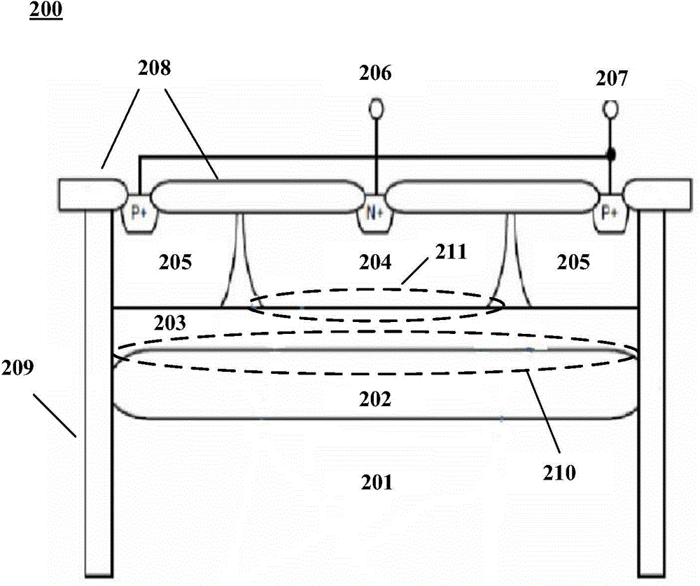
[0020] An embodiment of the present invention provides a semiconductor device, figure 2 is a schematic structural view of a semiconductor device according to Embodiment 1 of the present invention. Such as figure 2 As shown, the semiconductor device 200 includes:

[0021] A first N-type layer 202, which is formed on the semiconductor substrate 201;

[0022] A first P-type layer 203 formed on the first N-type layer 202;

[0023] A second N-type layer 204, which is formed on the first P-type layer 203;

[0024] A second P-type layer 205, which is formed on the first P-type layer 203;

[0025] a first electrode 206 connected to the second N-type layer 204; and

[0026] The second electrode 207 is connected to the second P-type layer 205 .

[0027] In this embodiment, the semiconductor device 200 may be any semiconductor device having the above structure, for example, the semiconductor device 200 may be a diode, a transistor or a laterally diffused metal oxide semiconductor...

Embodiment 2

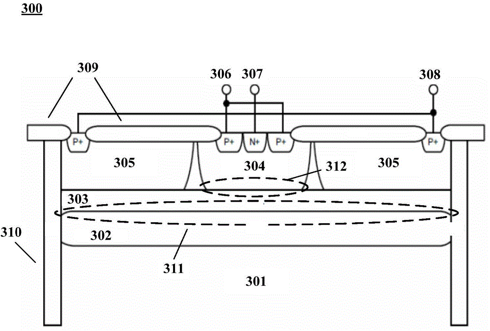
[0043] The embodiment of the present invention is described by taking the semiconductor device as a transistor as an example. image 3 It is a structural schematic diagram of the transistor of Example 2 of the present invention. Such as image 3 As shown, transistor 300 includes:

[0044] A first N-type layer 302 formed on the semiconductor substrate 301;

[0045] A first P-type layer 303 formed on the first N-type layer 302;

[0046] A second N-type layer 304 formed on the first P-type layer 303;

[0047] A second P-type layer 305 formed on the first P-type layer 303;

[0048] Emitter 306 and base 307, which are connected to the second N-type layer 304; and

[0049] The collector electrode 308 is connected to the second P-type layer 305 .

[0050] In this embodiment, the transistor 300 may further include a first oxide layer 309 and a second oxide layer 310 for electrically insulating the inside of the semiconductor device from the outside. For example, if image 3 As...

Embodiment 3

[0056] Embodiments of the present invention are described by taking a laterally diffused metal oxide semiconductor (LDMOS) semiconductor device as an example. Figure 4 It is a schematic structural diagram of a laterally diffused metal oxide semiconductor (LDMOS) according to Embodiment 3 of the present invention. Such as Figure 4 As shown, laterally diffused metal oxide semiconductor (LDMOS) 400 includes:

[0057] A first N-type layer 402 formed on the semiconductor substrate 401;

[0058] A first P-type layer 403 formed on the first N-type layer 402;

[0059] A second N-type layer 404 formed on the first P-type layer 403;

[0060] A second P-type layer 405 formed on the first P-type layer 403;

[0061] Gate 406 and source 407, which are connected to the second N-type layer 404; and

[0062] The base 408 is connected to the second P-type layer 405 .

[0063] In this embodiment, the laterally diffused metal oxide semiconductor (LDMOS) 400 may further include a first oxi...


PUM


Abstract

The embodiment of the invention provides a semiconductor device and electronic equipment. The semiconductor device comprises a first N-type layer formed on a semiconductor substrate, a first P-type layer formed on the first N-type layer, a second N-type layer formed on the first P-type layer, a second P-type layer formed on the first P-type layer, a first electrode connected with the second N-type layer and a second electrode connected with the second P-type layer. Through forming two PN junction areas with a wide range, a depletion layer area with a wide range can be formed when voltage is applied to the semiconductor device, the voltage-withstanding performance of the semiconductor device can be effectively improved, the thickness of the semiconductor device does not need to be added, the manufacturing process of the semiconductor device is simplified, and the manufacturing cost is saved.

Description

technical field [0001] The invention relates to the technical field of semiconductors, in particular to a semiconductor device and electronic equipment. Background technique [0002] When a voltage is applied to the semiconductor device, the PN junction of the semiconductor device is easily broken down as the voltage increases. Therefore, the withstand voltage performance of the semiconductor device is one of the important performances of the semiconductor device. figure 1 is a schematic diagram of the existing diode structure. Such as figure 1 As shown, the diode 100 includes a P-type substrate 101, a first N-type layer 102 formed on the P-type substrate 101, a second N-type layer 103 formed on the first N-type layer 102, and a second N-type layer 103 formed on the first N-type layer. 102 on the N-type layer 104 on both sides of the second N-type layer 103, the first oxide layer 105 formed on the upper part of the diode, the second oxide layer 106 formed on both sides of...

Claims


Application Information

Patent Timeline
Patent Type & Authority Applications(China)
IPC IPC(8): H01L29/861H01L29/06H01L29/78
Inventor 高桥健一郎
Owner SANKEN ELECTRIC CO LTD
Why Eureka
Try Eureka