A kind of LED chip structure and preparation method thereof

A chip structure and buffer layer technology, applied in semiconductor devices, electrical components, circuits, etc., can solve the problem of low hole injection efficiency, improve ohmic contact characteristics, increase hole injection efficiency, and reduce the width of the depletion layer. Effect

Active Publication Date: 2018-11-02
ZHIXIN SEMICON (HANGZHOU) CO LTD
View PDF7 Cites 0 Cited by
  • Summary
  • Abstract
  • Description
  • Claims
  • Application Information

AI Technical Summary

Problems solved by technology

[0004] The technical problem to be solved by the present invention is to provide a chip structure of LED and its preparation method, by inserting an insulating layer between the P-type semiconductor material and the electrode, thereby reducing the contact between the P-type semiconductor material and the metal. The length of the depletion region increases the hole concentration, increases the hole tunneling probability, reduces the contact resistance of the P-type semiconductor material / P-electrode, and improves the internal quantum efficiency and electro-optical conversion efficiency, thereby overcoming the existing technology. The doping efficiency of P-type semiconductor materials in LED devices is not high, and the defect of hole injection efficiency is low

Method used


Image

  • A kind of LED chip structure and preparation method thereof
  • A kind of LED chip structure and preparation method thereof
  • A kind of LED chip structure and preparation method thereof

Examples


Embodiment 1

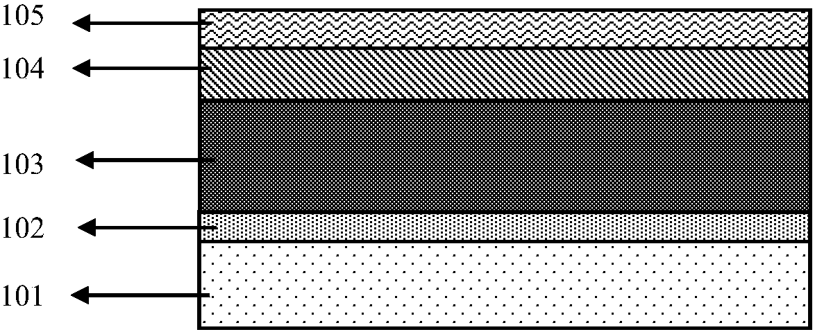
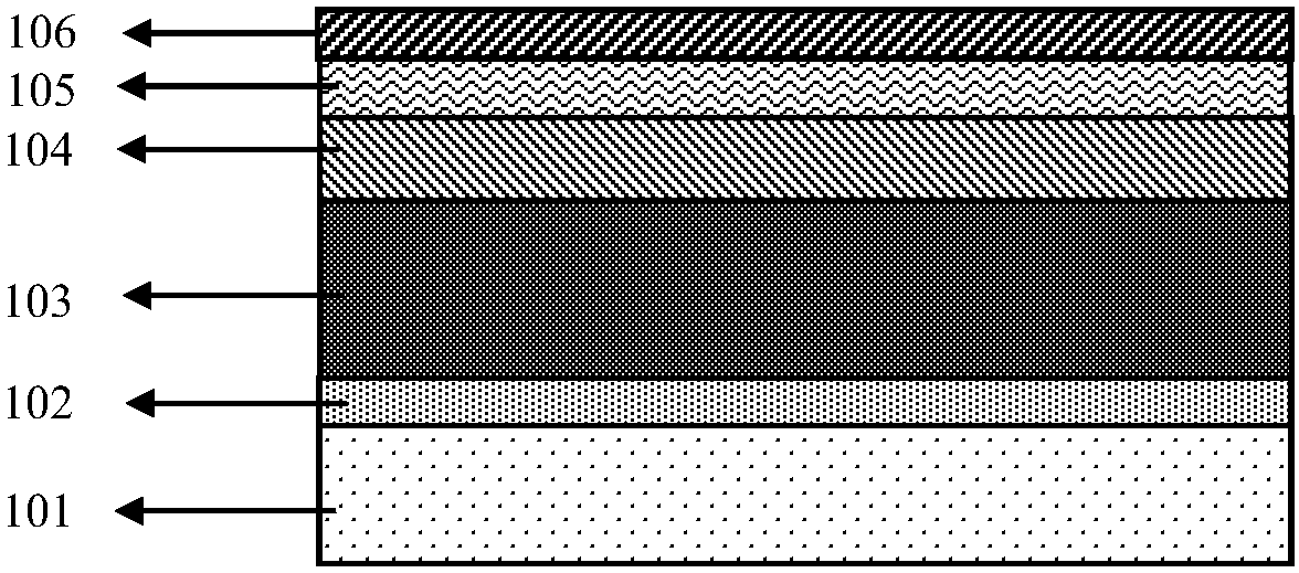
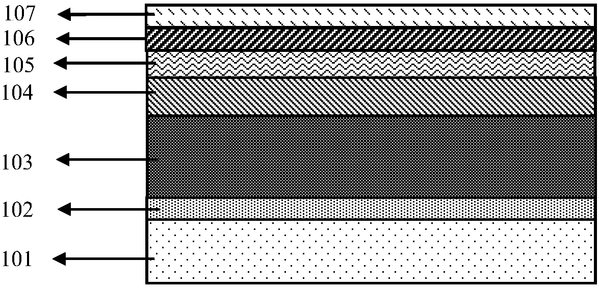
[0047] The chip structure of a kind of LED of this embodiment comprises substrate 101, buffer layer 102, N-type semiconductor material 103, N-type ohmic electrode 109 formed on N-type semiconductor material 103, multi-quantum well layer 104 in order from bottom to top , P-type semiconductor material 105, insulating layer 106, current spreading layer 107 and P-type ohmic electrode 108, wherein the insulating layer 106 is made of AlN with a thickness of 0.5nm, and the insulating layer 106 is a continuous film structure.

[0048] Among the above, the substrate 101 is sapphire; the material of the buffer layer 102 is InN, and the thickness is 10nm; the material of the N-type semiconductor material 103 is InN. 0.9 Ga 0.1 N, with a thickness of 2 μm; the material of the multi-quantum well layer 104 is InN / In 0.9 Ga 0.1 N, where the quantum barrier In 0.9 Ga 0.1 The thickness of N is 5nm, and the thickness of quantum well InN is 1nm; The material of P-type semiconductor material ...

Embodiment 2

[0059] The chip structure of a kind of LED of this embodiment comprises substrate 101, buffer layer 102, N-type semiconductor material 103, N-type ohmic electrode 109 formed on N-type semiconductor material 103, multi-quantum well layer 104 in order from bottom to top , P-type semiconductor material 105, insulating layer 106, current spreading layer 107 and P-type ohmic electrode 108, wherein the material used for insulating layer 106 is SiO 2 , with a thickness of 10 nm, the insulating layer 106 has a discontinuous film structure, and the discontinuous film structure is produced by photolithography.

[0060] Among the above, the substrate 101 is Si; the material of the buffer layer 102 is GaN, and the thickness is 30nm; the material of the N-type semiconductor material 103 is GaN, and the thickness is 5 μm; the material of the multi-quantum well layer 104 is In 0.25 Ga 0.75 N / GaN, where the thickness of the quantum barrier GaN is 26nm, and the quantum well In 0.25 Ga 0.75 ...

Embodiment 3

[0071] The chip structure of a kind of LED of this embodiment comprises substrate 101, buffer layer 102, N-type semiconductor material 103, N-type ohmic electrode 109 formed on N-type semiconductor material 103, multi-quantum well layer 104 in order from bottom to top , P-type semiconductor material 105, insulating layer 106, current spreading layer 107 and P-type ohmic electrode 108, wherein the insulating layer 106 is made of SiN with a thickness of 20nm, and the insulating layer 106 is a continuous film structure.

[0072] Among the above, the substrate 101 is SiC; the material of the buffer layer 102 is AlN, and the thickness is 50nm; the material of the N-type semiconductor material 103 is AlN, and the thickness is 8 μm; the material of the multi-quantum well layer 104 is Al 0.9 Ga 0.1N / AlN, where the thickness of the quantum barrier AlN is 50nm, and the quantum well Al 0.9 Ga 0.1 The thickness of N is 10nm; The material of P-type semiconductor material 105 is AlN, and ...


PUM


Abstract

The invention provides an LED chip structure and a preparation method thereof, and relates to a semiconductor device which has at least one potential jump barrier or surface potential barrier and is used specially for light emission. The LED chip structure comprises, from top to bottom, a substrate, a buffer layer, an N-type semiconductor material, a multi-quantum well layer, a P-type semiconductor material, an insulating layer, a current expanding layer, a P-type ohmic electrode and an N-type ohmic electrode in order. With a thickness of 0.5-20 nm, the insulating layer is made of undoped ALN, AL2O3, SiO2, Si3N4, diamond, LiF or PMMA. By insertion of the insulating layer, the length of a depletion region at the part where the P-type semiconductor material and metal are contacted is decreased, the hole concentration is enhanced, the hole tunneling rate is increased, the contact resistance of the P-type semiconductor material / P-type electrode is reduced, the internal quantum efficiency and electro-optic conversion efficiency are improved, and the defects of the prior art of relatively low doping efficiency of P-type semiconductor materials in LED devices and low hole injection efficiency are solved.

Description

technical field [0001] The technical solution of the invention relates to a semiconductor device specially suitable for light emission with at least one potential jump barrier or surface barrier, specifically a LED chip structure and its preparation method. Background technique [0002] Based on nitride semiconductor LED technology, it plays an important role in slowing down global warming and improving the living environment. In the past 30 years, nitride semiconductor LED technology has achieved unprecedented development and has important application value in many fields, such as Display, lighting, communication, biomedicine and anti-counterfeiting detection and other technical fields. [0003] In order to further increase the application space of LEDs, an improved internal quantum efficiency is required. Studies have found that compared with electrons in LED devices, the mobility of holes is lower and the effective mass is larger, so the injection efficiency of holes is ...

Claims


Application Information

Patent Timeline
Patent Type & Authority Patents(China)
IPC IPC(8): H01L33/14H01L33/00
CPCH01L33/007H01L33/14
Inventor 张紫辉张勇辉毕文刚徐庶耿翀
Owner ZHIXIN SEMICON (HANGZHOU) CO LTD
Why Eureka
Try Eureka