Double-layer chip scale package (CSP) light source and manufacturing method thereof

A chip-level packaging and double-layer structure technology, applied in the field of lighting, can solve the problems of exceeding the temperature resistance limit of silica gel, short life, and incomplete colloid, and achieve the effect of solving the problem of color coordinate change, long service life, and good temperature resistance

Inactive Publication Date: 2016-09-14
江西兆驰光元科技股份有限公司
View PDF4 Cites 21 Cited by
  • Summary
  • Abstract
  • Description
  • Claims
  • Application Information

AI Technical Summary

Problems solved by technology

Ordinary five-sided CSP light source, because the phosphor powder is evenly dispersed in the fluorescent glue, the phosphor powder is excited by the blue light emitted by the light-emitting chip, and generates new light waves while releasing a large amount of heat. Due to the limited thermal conductivity of silica gel, the distance from the light-emitting chip is close Phosphor powder particles, the heat generated by it is easy to conduct to the substrate through the light-emitting chip; but the heat generated by the phosphor particles far away from the light-emitting chip is blocked by silica gel, and it is difficult to conduct to the light-emitting chip and the substrate; after the light source works for a long time, The undissipated heat continues to accumulate, eventually exceeding the temperature resistance limit of silica gel, resulting in colloidal fragmentation of the light source, resulting in the following problems: (1) The fluorescent colloid is easily damaged during use, and the colloid is incomplete, resulting in changes in the color coordinates of the light source ; (2) Under long-term work, the heat generated by CSP is difficult to conduct to the substrate, resulting in the light source being prone to fragmentation of fluorescent colloid, failure of the light source, and short life

Method used


Image

  • Double-layer chip scale package (CSP) light source and manufacturing method thereof
  • Double-layer chip scale package (CSP) light source and manufacturing method thereof
  • Double-layer chip scale package (CSP) light source and manufacturing method thereof

Examples


Embodiment Construction

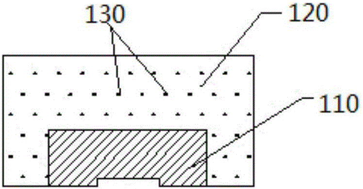
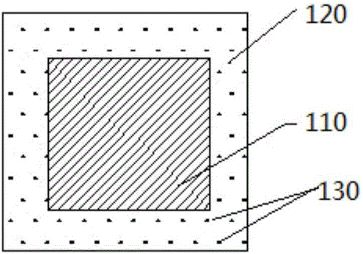
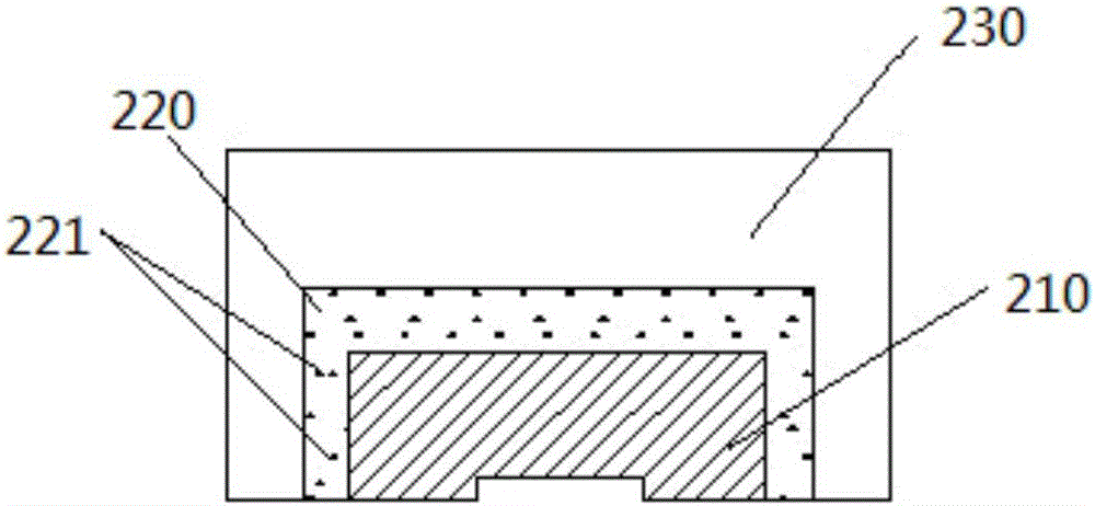
[0028] see Figure 3-5 A light source with a double-layer chip-scale package of the present invention includes a light-emitting chip 210, a fluorescent adhesive layer 220 surrounding the light-emitting chip, and a transparent adhesive layer 230 surrounding the fluorescent adhesive layer.

[0029] The fluorescent adhesive layer 220 in the double-layer structure chip-level packaging light source of the present invention is a thin fluorescent adhesive film, since the phosphor powder is distributed in a very thin adhesive film (the thickness of the thin adhesive film is in the range of 50-150um), and it is close to the light-emitting chip, The heat generated is easily conducted to the substrate through the chip, so its temperature resistance is better. Phosphor powder 221 is uniformly mixed in the fluorescent adhesive layer 220 .

[0030] The transparent adhesive layer 230 is a silica gel layer, and the silica gel at the outermost periphery can protect the fluorescent layer from ...


PUM


Abstract

The invention provides a double-layer chip scale package (CSP) light source. The light source comprises a luminous chip, a fluorescent gel layer surrounding the luminous chip, and a transparent gel layer surrounding the fluorescent gel layer. A manufacturing method of the double-layer CSP light source comprises the following steps: (1) the luminous chip is placed on a carrier plate; (2) the luminous chip is surrounded by fluorescent gel, so that the fluorescent gel layer is formed; (3) the fluorescent gel layer is packaged by the transparent gel layer; (4) baking curing is carried out to form the double-layer CSP light source. The double-layer CSP light source and the manufacturing method thereof provided by the invention have the advantages that fluorescent powders are distributed in a super-thin gel film and close to the luminous chip, so that generated heat can be easily conducted to a substrate through the chip, and higher temperature resistance can be further achieved; the fluorescent layer can be prevented from damage through the outermost silica gel, so that the problem of chromaticity coordinate changes of an ordinary five-sided CSP light source is solved.

Description

【Technical field】 [0001] The invention relates to the lighting field, in particular to a double-layer structure chip-scale packaging light source and a manufacturing method thereof. 【Background technique】 [0002] The new chip-scale package LED light source (CSP light source) based on flip-chip is equipped with electrodes on the bottom of the chip, and the colloid is directly packaged on the upper surface and side of the chip, so that the electrodes on the bottom surface are exposed. Since this packaging structure has no support or substrate , can reduce packaging cost. Existing chip-scale packaged light sources usually adopt five-sided light emitting, that is, both the top surface and the four sides of the LED can emit light. see figure 1 and figure 2 , the common five-sided CSP (Chip Scale Package, Chip Scale Package) light source is surrounded by the fluorescent colloid 120 containing the phosphor powder 130 to surround the light-emitting chip 110 , and there is no pr...

Claims


Application Information

Patent Timeline
Patent Type & Authority Applications(China)
IPC IPC(8): H01L33/50H01L33/54H01L33/56H01L33/64
CPCH01L33/507H01L33/505H01L33/54H01L33/56H01L33/642H01L2933/0041H01L2933/005
Inventor 周波何至年唐其勇
Owner 江西兆驰光元科技股份有限公司
Why Eureka
Try Eureka