Manufacturing method and apparatus of black silicon cell

A manufacturing method and a manufacturing device technology, which are applied in the field of PECVD coating of black silicon batteries, can solve problems such as light color, yellowing around, and easy-to-protrude surface grains, so as to achieve uniform surface color and improve quality

Active Publication Date: 2016-09-21
ZHEJIANG JINKO SOLAR CO LTD +1
View PDF6 Cites 2 Cited by
  • Summary
  • Abstract
  • Description
  • Claims
  • Application Information

AI Technical Summary

Problems solved by technology

Using diamond sheet to make black silicon battery can effectively reduce the production cost, but because the diamond sheet itself is relatively bright, its surface grains are easy to stand out, and the surrounding color caused by the PECVD process is lighter, and it is easy to cause black silicon battery after making it. Poor appearance of black silicon components
[0004] Due to RIE and PECVD equipment, RIE will cause a slight blue edge on the silicon wafer, and PECVD will cause a lighter

Method used


Image

  • Manufacturing method and apparatus of black silicon cell
  • Manufacturing method and apparatus of black silicon cell

Examples


Embodiment Construction

[0036] As mentioned in the background technology section, the existing PECVD equipment will cause the surrounding color of the silicon wafer to be lighter (film thickness), and the color of the black silicon battery to be darker. Can cause chromatic aberration at the edges of black-backed components.

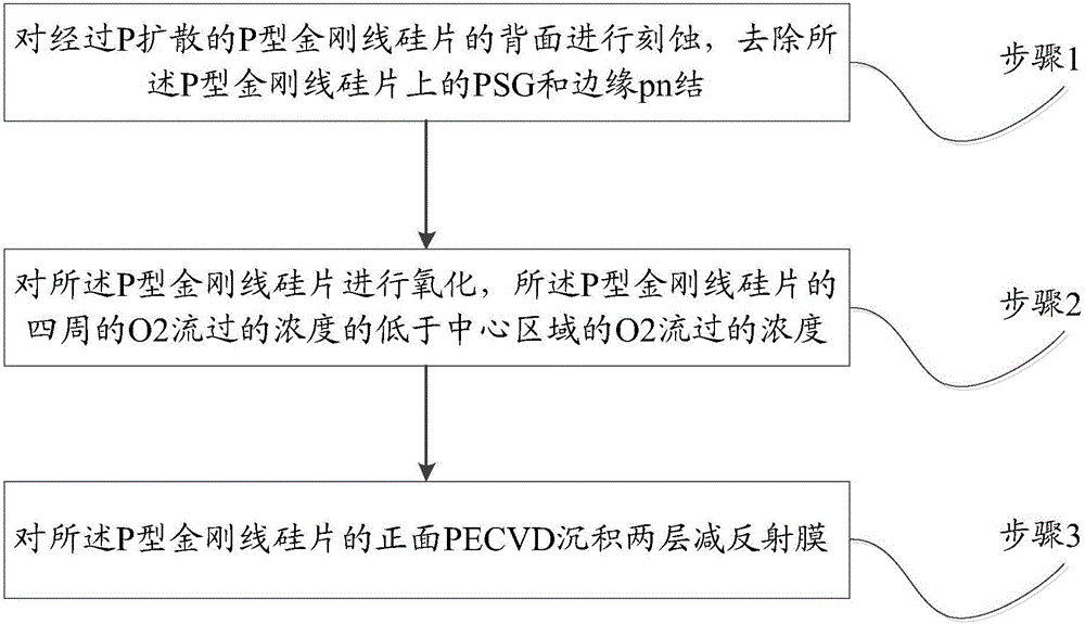
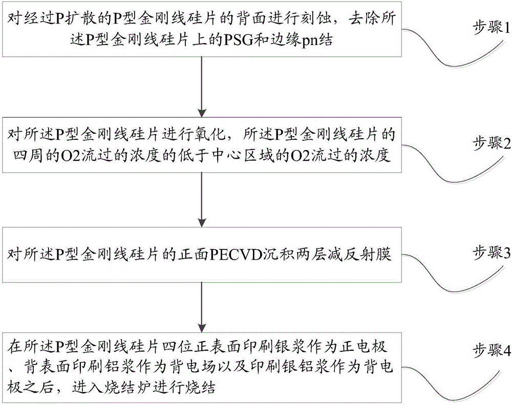
[0037] Based on this, an embodiment of the present invention provides a method for manufacturing a black silicon battery, including:

[0038] Step 1, etching the back side of the P-type diamond wire silicon wafer after P diffusion, and removing the PSG and edge pn junction on the P-type diamond wire silicon wafer;

[0039] Step 2, oxidizing the P-type diamond wire silicon wafer, the concentration of O2 flowing around the P-type diamond wire silicon wafer is lower than the concentration of O2 flowing through the central region;

[0040] Step 3, depositing two layers of anti-reflection films by PECVD on the front side of the P-type diamond wire silicon wafer.

[0041] In additio...


PUM

PropertyMeasurementUnit
Thicknessaaaaaaaaaa
Thicknessaaaaaaaaaa

Abstract

The invention discloses a manufacturing method and apparatus of a black silicon cell. The manufacturing method includes the steps: 1) etching the back of a P type diamond wire silicon chip which is processed through P diffusion, and removing the PSG and the edge pn junction on the P type diamond wire silicon chip; 2) oxidizing the P type diamond wire silicon chip, wherein the concentration of the O2 of the surrounding, flowed by O2, of the P type diamond wire silicon chip is lower than the concentration of the O2 of the central area, flowed by O2, of the P type diamond wire silicon chip; and 3) depositing two layers of anti-reflection films on the front PECVD of the P type diamond wire silicon chip. As the manufacturing method and apparatus of a black silicon cell enable the thickness of the oxide layer deposited at the central position of the diamond wire silicon chip to be higher than the thickness of the surrounding during the oxidation process and enable the thickness of the surrounding of the two layers of anti-reflection films to be higher than the thickness of the central area during the subsequent process of deposition of the two layers of anti-reflection films on the PECVD, the film thickness of the surface of the diamond wire silicon chip is uniform; the color of the diamond wire silicon chip is uniform; and the quality of the P type diamond wire silicon chip is improved.

Description

technical field [0001] The invention relates to the field of photovoltaic module manufacturing, in particular to a PECVD coating method and device for black silicon cells. Background technique [0002] PECVD equipment will cause the color around the silicon wafer to be lighter (film thickness), and the color of the black silicon cell to be darker. Therefore, after PECVD of the black silicon cell, there will be a significant color difference between the periphery and the center, and this color difference will cause color difference at the edge of the black backplane component. . [0003] Diamond wire cutting has the advantages of fast cutting speed, high precision, and low material loss. Therefore, compared with mortar wire cutting silicon ingots or rods, its production cost can be greatly reduced, and it has great application prospects. Using diamond sheet to make black silicon battery can effectively reduce the production cost, but because the diamond sheet itself is relat...

Claims


Application Information

Patent Timeline
IPC IPC(8): H01L31/18
CPCH01L31/02168Y02P70/50
Inventor 叶飞蒋方丹金浩
Owner ZHEJIANG JINKO SOLAR CO LTD
Why Eureka
Try Eureka