
Preparation method of metal gate

A metal gate and metal filling technology, used in semiconductor/solid-state device manufacturing, semiconductor devices, electrical components, etc., can solve problems such as over-polishing, different grinding rates, and butterfly-shaped depressions

Active Publication Date: 2016-10-05
SEMICON MFG INT (SHANGHAI) CORP +1
View PDF3 Cites 0 Cited by
  • Summary
  • Abstract
  • Description
  • Claims
  • Application Information

AI Technical Summary

Problems solved by technology

Therefore, when grinding, the grinding rate of each grinding area is not the same, which can easily lead to the phenomenon of over polish (over polishing) and bridge (bridging), and it is also easy to form butterfly-shaped depressions in the area near the sample grid. what people in the field don't want to see

Method used


Image

  • Preparation method of metal gate
  • Preparation method of metal gate
  • Preparation method of metal gate

Examples


preparation example Construction

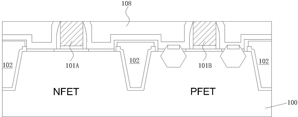
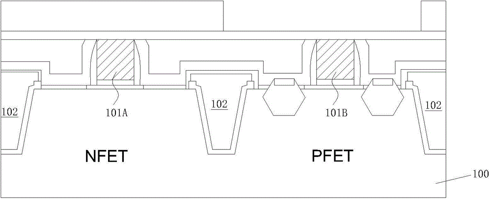
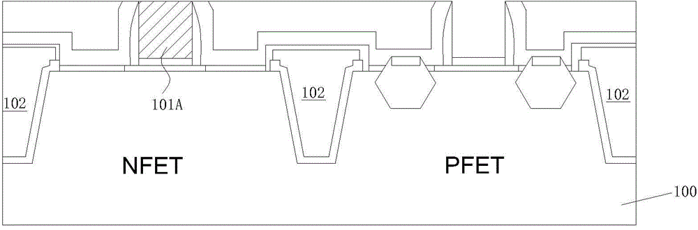
[0033] A method for preparing a metal grid, referring to Figures 3a-3e shown, including the following steps:

[0034] Step S1, providing a substrate, the surface of the substrate is covered with a dielectric layer (not shown in the figure), a first gate groove and a second gate groove are formed in the dielectric layer, and a first sample gate 101A is arranged in the first gate groove , the second sample grid 101B is disposed in the second grid groove; the height of the first sample grid is smaller than the thickness of the dielectric layer, and the height of the second sample grid is equal to the thickness of the dielectric layer.

[0035] Wherein, an N-MOSFET region (such as P-well) and a P-MOSFET region (such as N-well) are arranged in the substrate, and the N-MOSFET region and the P-MOSFET region are separated by a shallow trench isolation structure. isolation. The shallow trench isolation structure is that the trench is filled with an insulating material such as oxide,...


PUM


Abstract

The invention relates to the technical field of semiconductor preparation and specifically provides a preparation method of a metal gate. The method is an HKMG preparation method based on gate last and is characterized in that the sample gate of one device region is thinned, a hard mask layer is prepared on the top part thereof, then in the metal gate preparing process of other device regions and in the grinding process, the hard mask layer can effectively protect the below sample gate against damages, and the evenness of the surface of the device after grinding is further improved.

Description

technical field [0001] The present invention relates to the technical field of semiconductor manufacturing, specifically, to the metal gate-last process, and specifically provides a method for preparing a metal gate. Background technique [0002] With the continuous development of technology, semiconductor technology has penetrated into various fields of life, such as aerospace, medical devices, and mobile phone communications, which cannot be separated from chips prepared by semiconductors. [0003] In the past, many chips used silicon dioxide as the gate dielectric, but starting from 65nm, due to the small technology node, the gate dielectric cannot continue to be shortened and thinned. At the same time, as the size of the transistor continues to shrink, the source The distance between the electrode and the drain is also getting smaller and smaller, which is easy to cause the short channel effect. Therefore, in view of the above problems, the HKMG (High-K Metal Gate, high...

Claims


Application Information

Patent Timeline
Patent Type & Authority Applications(China)
IPC IPC(8): H01L21/8238H01L21/28
Inventor 赵简曹轶宾王杭萍
Owner SEMICON MFG INT (SHANGHAI) CORP
Features
  • Generate Ideas
  • Intellectual Property
  • Life Sciences
  • Materials
  • Tech Scout
  • Unparalleled Data Quality
  • Higher Quality Content
  • 60% Fewer Hallucinations
Learn More