Logical block address-to-physical block address mapping method for high-capacity solid-state disk

A technology of logic mapping and solid-state hard disk, which is applied in the direction of electrical digital data processing and instruments, and can solve problems such as complex design, large mapping table, and high power consumption

Active Publication Date: 2016-10-12
BEIJING KUANGEN NETWORK TECH
View PDF3 Cites 8 Cited by
  • Summary
  • Abstract
  • Description
  • Claims
  • Application Information

AI Technical Summary

Problems solved by technology

[0004] In the design of large-capacity solid-state drives, a prominent problem is that the mapping table may be too large
Larger mapping table means larger double-ra...

Method used


Image

  • Logical block address-to-physical block address mapping method for high-capacity solid-state disk

Examples


Embodiment Construction

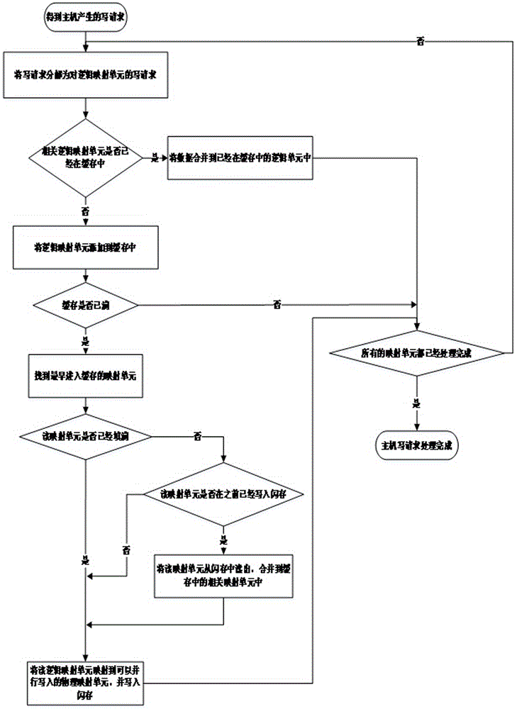
[0029] The preferred embodiments of the present invention will be described below in conjunction with the accompanying drawings. It should be understood that the preferred embodiments described here are only used to illustrate and explain the present invention, and are not used to limit the present invention.

[0030] Such as figure 1 As shown, a method for mapping a large-capacity solid state drive from a logical address to a physical address includes the following steps:

[0031] Step 1. Obtain the write request generated by the host;

[0032] Step 2. Decompose the write request obtained above into write requests to the logical mapping unit, and go to step 3;

[0033] Step 3. Determine whether the above logical mapping unit is already in the cache. If the logical mapping unit is in the cache, merge the write request data for the logical mapping unit decomposed in step 2 into the logical mapping unit in the cache, and go to step 9. If the logical mapping unit is not in the cache, go...


PUM


Abstract

The invention discloses a logical block address-to-physical block address mapping method for a high-capacity solid-state disk. The method comprises the steps of defining that a logical mapping unit is composed of a plurality of logic blocks; decomposing a write request of a host into a write request for the logical mapping unit; judging whether the logical mapping unit is in a cache or not, adding the logical mapping unit to the cache, and judging whether the cache is full or not; judging whether the logical mapping unit entering the cache at the earliest is written in the cache or not if the cache is full; mapping the logical mapping unit entering the cache at the earliest to a physical mapping unit capable of realizing parallel write, writing the logical mapping unit into a flash memory if the logical mapping unit is not written into the cache; reading the mapping unit from the flash memory if the mapping unit is written into the flash memory previously, combining the mapping unit with the data in the cache, mapping the combined logical mapping unit to the physical mapping unit capable of realizing parallel write, and writing the logical mapping unit into the flash memory. The size of a mapping table is controlled.

Description

[0001] technical field [0002] The invention relates to the field of data storage, in particular to a large-capacity solid-state hard disk logical address-to-physical address mapping method. Background technique [0003] Currently, NAND flash-based solid-state drives (SSDs) need to map the logical address (LBA) used by the host to the actual physical address of the flash. Usually, in order to improve the throughput of reading and writing, flash memory chips are placed on different channels (Channels), and there are usually several Targets in the flash memory chip, each Target has several LUNs, and each LUN has Several Planes, each Plane will have several blocks (Block), and each Block will have several pages (Page). Blocks and pages located on different channels, different chips, different targets, different LUNs and different planes can be read and written in parallel. So the physical address of flash memory includes channel number, chip number, Target address, LUN addre...

Claims


Application Information

Patent Timeline
IPC IPC(8): G06F13/40
CPCG06F13/404
Inventor 孙易安
Owner BEIJING KUANGEN NETWORK TECH
Why Eureka
Try Eureka