Rapid turning-off silicon-on-insulator-lateral insulated gate bipolar transistor

A bipolar transistor and silicon-on-insulator technology, which is applied in electric solid state devices, semiconductor devices, semiconductor/solid state device components, etc., can solve the problem of increasing device area and complexity, insufficient withstand voltage, and reducing device on-current density. and other problems, to achieve the effects of low on-voltage drop, short off-time, and short current drop time

Active Publication Date: 2016-10-12
SOUTHEAST UNIV
View PDF4 Cites 4 Cited by
  • Summary
  • Abstract
  • Description
  • Claims
  • Application Information

AI Technical Summary

Problems solved by technology

For Dual LIGBT, when the device is turned off, the second gate will be opened to provide a path for electrons. This structure requires additional control circuits, and it increases the device area and complexity.
Other structures that reduce the off-time will also bring about problems such as reducing the on-current density of the device or insufficient withstand voltage.

Method used


Image

  • Rapid turning-off silicon-on-insulator-lateral insulated gate bipolar transistor
  • Rapid turning-off silicon-on-insulator-lateral insulated gate bipolar transistor
  • Rapid turning-off silicon-on-insulator-lateral insulated gate bipolar transistor

Examples


Embodiment Construction

[0023] Combine below figure 1 , figure 2 , image 3 , Figure 4 , the present invention is described in detail:

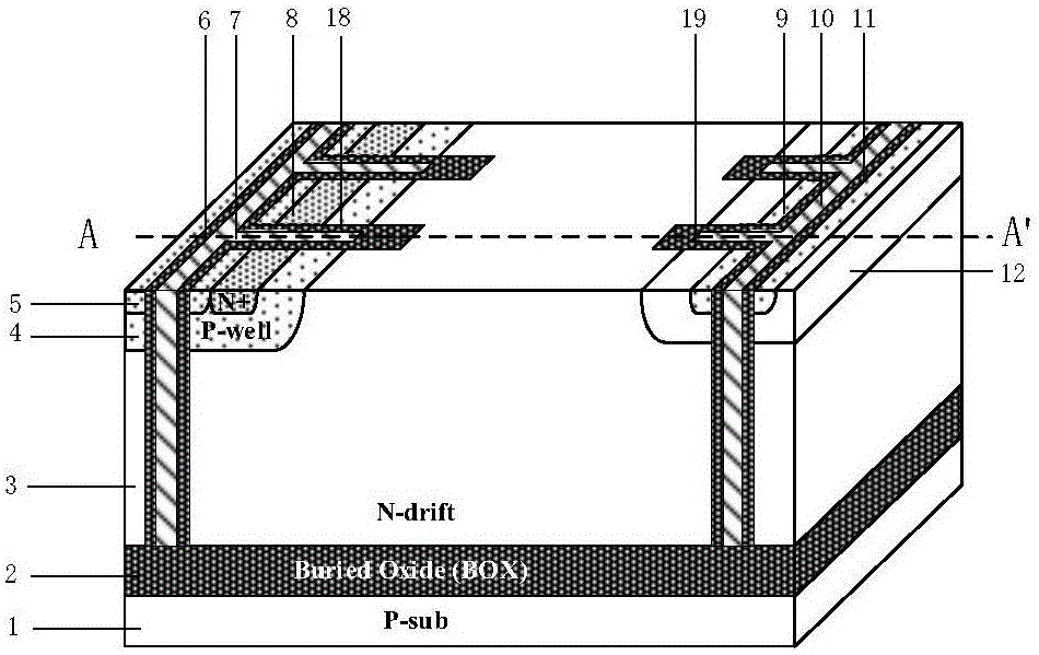
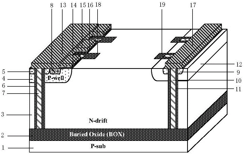
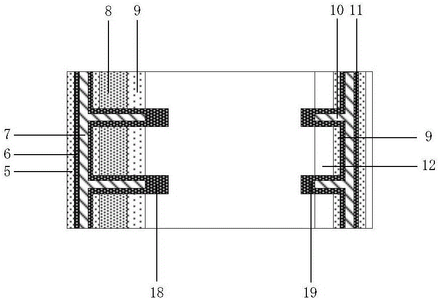
[0024] A fast turn-off silicon-on-insulator lateral insulated gate bipolar transistor device, comprising: a P-type substrate 1, a buried oxygen 2 is arranged on the P-type substrate 1, and an N-type drift region 3 is arranged on the buried oxygen 2 , N-type buffer region 12 and P-type well region 4 are respectively arranged on both sides of N-type drift region 3, in N-type buffer region 12, there is heavily doped P-type collector region 9, heavily doped P-type An anode metal 17 is connected to the collector region 9, and a heavily doped P-type emitter region 5 and a heavily doped N-type emitter region 8 are arranged in the P-type well region 4, wherein the heavily doped N-type emitter region The pole region 8 is inside the heavily doped P-type emitter region 5, the heavily doped N-type emitter region 8 and the heavily doped P-type emitter region 5 are connect...


PUM


Abstract

A fast turn-off silicon-on-insulator lateral insulated gate bipolar transistor device, the semiconductor has: a buried oxygen on a P-type substrate, an N-type drift region on the buried layer, a P-type well region and a N-type buffer area, in the N-type buffer area, there is a heavily doped P-type collector region, in the P-type well region, there are heavily doped P-type emitter regions and N-type emitter regions, in the P-type well region There is a gate oxide layer on the surface, and a polysilicon layer on it. In the heavily doped P-type emitter region, there is a first vertical groove that is as deep as the buried oxygen. A lateral trench extending to the drift region, a second vertical trench is provided in the heavily doped P-type collector region and its depth is as deep as buried oxygen, and the above-mentioned trench partially expands inward to form second transverse trenches with equal spacing The groove extends to the drift region, and all the above grooves are filled with polysilicon wrapped with a pressure-resistant medium, and the filler located in the drift region is a pressure-resistant medium.

Description

technical field [0001] The invention mainly relates to the technical field of power semiconductor devices, and is a novel fast-turn-off silicon-on-insulator lateral insulated gate bipolar transistor, which is especially suitable for monolithic integrated power chips and used to realize accurate control of various circuit systems. Background technique [0002] Silicon-on-insulator lateral insulated gate bipolar transistor (SOI-LIGBT) is a high-speed, power bipolar transistor (BJT) with high current density of power-collecting SOI lateral double-diffused metal-oxide-semiconductor field-effect transistor (LDMOSFET) It is a power device with the advantages of SOI full dielectric isolation, so it has the advantages of simple driving, easy protection, and high switching frequency. Therefore, based on the above advantages, SOI-LIGBT is now widely used in various high-power power electronic equipment. [0003] Since SOI-LIGBT is usually used as a power switching device in integrated...

Claims


Application Information

Patent Timeline
Patent Type & Authority Applications(China)
IPC IPC(8): H01L29/739H01L29/08H01L23/50
CPCH01L29/7393H01L23/50H01L29/0804H01L29/0821
Inventor 孙伟锋黄薛佺张龙祝靖陆生礼时龙兴
Owner SOUTHEAST UNIV
Why Eureka
Try Eureka