Semiconductor conic laser device

A laser and semiconductor technology, applied in the structure of optical waveguide semiconductors, can solve the problems of poor beam quality, complex fabrication, poor heat dissipation of tapered lasers, etc., and achieve the effect of reducing current density, good beam quality, and avoiding poor heat dissipation.

Inactive Publication Date: 2016-10-12
XI'AN INST OF OPTICS & FINE MECHANICS - CHINESE ACAD OF SCI
View PDF5 Cites 8 Cited by
  • Summary
  • Abstract
  • Description
  • Claims
  • Application Information

AI Technical Summary

Problems solved by technology

[0006] The present invention proposes a new cone-shaped laser (surface electrode structure), which not only overcomes the problem of poor beam quality of the existing cone-shaped laser with integrated electrodes when high current is injected, but also avoids the existing cone-shaped electrode separation. Problems such as poor heat dissipation and complex fabrication of shaped lasers

Method used


Image

  • Semiconductor conic laser device
  • Semiconductor conic laser device
  • Semiconductor conic laser device

Examples


Embodiment Construction

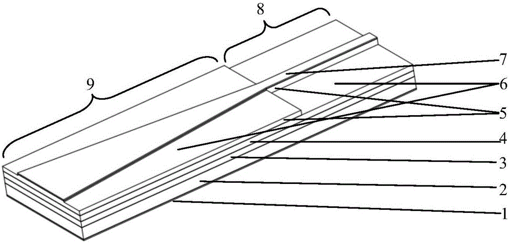
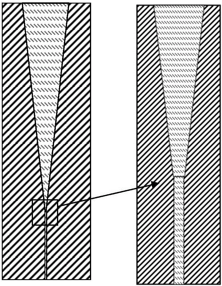
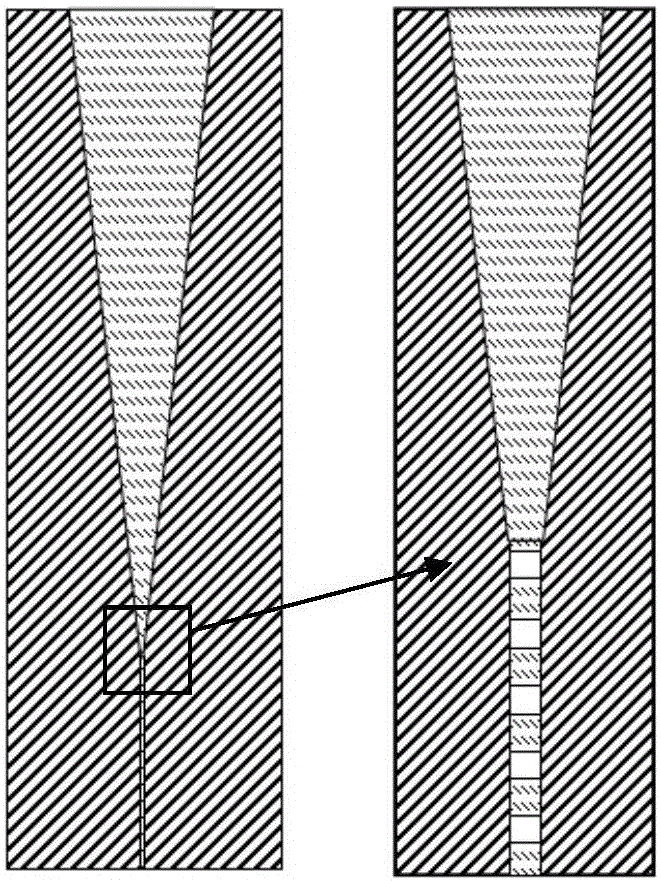
[0027] Such as figure 1 As shown, from bottom to top, it includes N-face electrode, N-face substrate, N cladding layer, confinement layer, P cladding layer, and P-face electrode. The length of the laser is 4mm and the width is 1mm. The laser is divided into a ridge area and an amplification area as a whole. The length of the ridge waveguide part is 1mm and the width is 0.005mm. The surface width is 0.32mm. The surface of the ridge waveguide is composed of ten small electrodes. The length of each electrode is 0.05mm, the width is 0.005mm, and the distance between the electrodes is 0.05mm. The layers are exactly the same.

[0028] On the planes on both sides of the electrode on the P surface, an insulating coating is provided to prevent current from directly flowing out of the substrate without passing through the active region. Wherein, the insulating plating layer in the ridge-shaped area is located on the surface of the restriction layer at the corresponding position, and t...


PUM


Abstract

The invention provides a novel semiconductor conic laser device, namely a surface electrode structure, solves a problem of poor light beam quality during high current injection of an integrated electrode conic laser device in the prior art and further solves problems of poor heat radiation and complex manufacturing process of a separated electrode conic laser device in the prior art. According to the semiconductor conic laser device, a ridge-type waveguide surface electrode is cut into segments, a part of the electrode on a ridge-type waveguide surface is removed, an electrode area of the ridge-type waveguide surface is reduced, so current components injected into a ridge-type waveguide can be reduced when an anode power source electrode is integrally crimped at a ridge-type zone portion of a P-surface electrode, current density of an active zone of the ridge-type waveguide is reduced, and light beam quality of the conic laser device is improved under the condition of high current injection. The novel semiconductor conic laser device is advantaged in that advantages of two types of conic laser devices in the prior art are integrated, and properties of low injection current, simple manufacturing, good heat radiation and good light beam quality of the ridge-type waveguide are realized.

Description

technical field [0001] The invention belongs to the field of semiconductor optoelectronics and relates to a semiconductor cone laser. Background technique [0002] High-power, high-brightness semiconductor lasers are widely used in medical equipment, material processing and other fields, and their competitiveness in the market has gradually increased in recent years. The brightness of a semiconductor laser refers to the optical power per unit area and unit divergence angle of the output beam, which is determined by the output optical power and beam quality of the semiconductor laser. When the gain length of the semiconductor laser remains unchanged, increasing the width of the light-emitting unit of the semiconductor laser can increase the area of ​​the active region and increase the output power, but the thermal effect and carrier focusing effect of the larger gain region cause higher-order modes. Laser and filament effects reduce the beam quality of the light output unit....

Claims


Application Information

Patent Timeline
Patent Type & Authority Applications(China)
IPC IPC(8): H01S5/22
CPCH01S5/22
Inventor 李秀山王贞福杨国文
Owner XI'AN INST OF OPTICS & FINE MECHANICS - CHINESE ACAD OF SCI
Why Eureka
Try Eureka