
CMOS (Complementary Metal Oxide Semiconductor) integrated circuit terahertz source applied to terahertz skin imaging field
An integrated circuit and skin imaging technology, applied in the field of terahertz skin imaging, can solve the problems of low surface mobility and low quality factor of passive devices, achieve high conversion gain frequency multiplication, wide locking range, and overcome process errors.
Patent Information
- Authority / Receiving Office
- CN · China
- Current Assignee / Owner
- Publication Date
- 2016-10-12
Smart Images
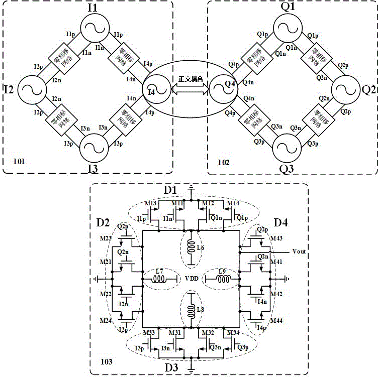
Figure 1 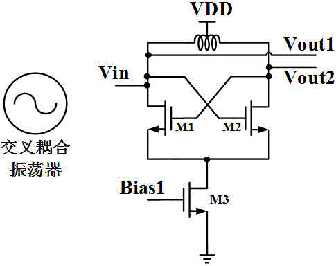
Figure 2 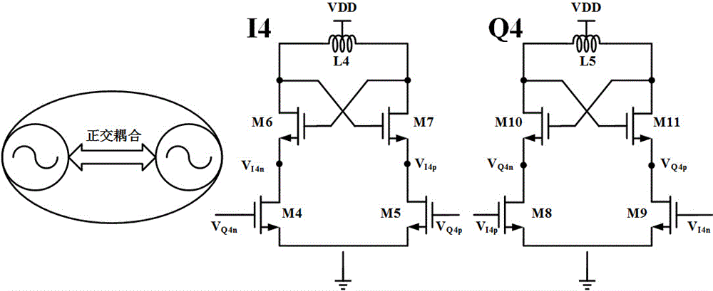
Figure 3
Abstract
Description
technical field
[0001] The invention belongs to the technical field of terahertz skin imaging, and in particular relates to a CMOS integrated circuit terahertz source. Background technique
[0002] With the development of terahertz technology, terahertz-detection medicine (terahertz-LabMed) is currently receiving great attention. Terahertz wave imaging technology has more unique and more applicable physical characteristics, and the photon energy is low, so it will not be harmful to living things. Molecules, biological cells and tissues produce harmful ionization, the radiation dose is almost zero, and the damage to the human body is very small. It is especially suitable for biopsy of biological tissues and provides a new and reliable technical method for human skin imaging research.
[0003] Thanks to the reduction of device size and the further development of technology, CMOS integrated circuits have also entered the millimeter wave and even terahertz frequency bands, makin...
Examples
Embodiment Construction
[0015] The CMOS integrated circuit terahertz source of the present invention applied in the field of terahertz skin imaging will be described in detail below with reference to the accompanying drawings.
[0016] The circuit structure of the present invention is as attached figure 1 As shown, it is divided into three modules 101, 102 and 103, of which two modules 101 and 102 are 8 cross-coupled oscillator circuits, module 101 is composed of 4 cross-coupled oscillators I1, I2, I3 and I4, and I1 There are zero phase shift network connections between I2, I2 and I3, I3 and I4, I4 and I1 respectively; module 102 is composed of 4 cross-coupled oscillators Q1, Q2, Q3 and Q4, and Q1 and Q2, Q2 and Q3 , Q3 and Q4, Q4 and Q1 are respectively connected by a zero-phase-shift network; I4 and Q4 are connected through quadrature coupling.
[0017] Among them, the internal structures of I1, I2, I3 and Q1, Q2, Q3 are exactly the same, such as figure 2 As shown, the drains of the NMOS transis...