Array substrate, method for manufacturing same and display device

An array substrate and black matrix technology, applied in the field of array substrate and its preparation method and display device, can solve the problems of array substrate film surface quality and abnormal function, pre-correction and adjustment, interference positioning, etc., to improve display quality and performance , Improving exposure quality and performance, improving the effect of preparation quality

Active Publication Date: 2016-10-26
BOE TECH GRP CO LTD +1
View PDF5 Cites 4 Cited by
  • Summary
  • Abstract
  • Description
  • Claims
  • Application Information

AI Technical Summary

Problems solved by technology

[0003] However, due to the high optical density OD of the black matrix BM, after the BM photoresist is directly coated on the Array substrate, the exposure light commonly used by the exposure equipment cannot penetrate the BM layer, which will interfere with the BM mask on the Array substrate. The identification, capture and positioning of the alignment mark Mark on the substrate makes it impossible for the black matrix mask BM Mask to be accurately aligned with the Array substrate, so that the exposure machine can only rely on the equipment itself and the Array substrate and the black matrix mask BM Mask The physical and mechanical alignment of the above-mentioned alignment mark Mark cannot be pre-corrected and adjusted, which greatly reduces the exposure accuracy of BM, resulting in a large error in the total pitch TP (Total Pitch) of the black matrix pattern BM Pattern on the array substrate, that is, BM The difference between the actual value of pattern exposure and the design value CD Bias is relatively large, which eventually leads to abnormal film surface quality and function of the array substrate

Method used


Image

  • Array substrate, method for manufacturing same and display device
  • Array substrate, method for manufacturing same and display device
  • Array substrate, method for manufacturing same and display device

Examples


Embodiment 1

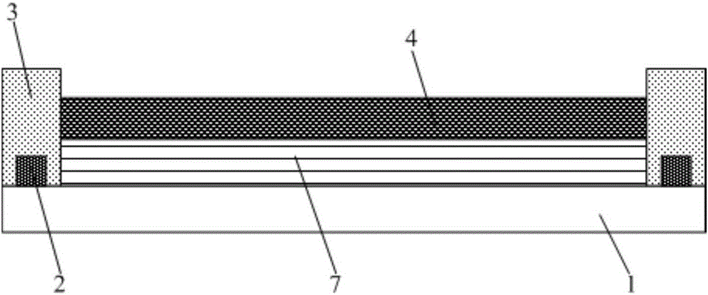
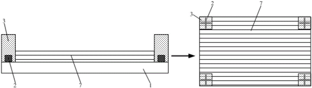
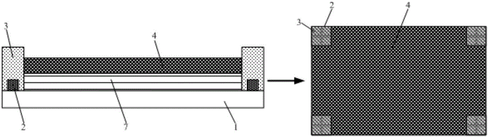
[0040] This embodiment provides a method for preparing an array substrate, such as Figure 1-Figure 7 As shown, it includes: step S1 : forming an alignment mark covering layer 3 on the region corresponding to the alignment mark 2 formed on the substrate 1 by using a patterning process. Step S2: forming a black matrix film 4 on the substrate 1 except for the alignment mark 2 . Step S3: removing the alignment mark covering layer 3 by exposure to expose the alignment mark 2 . Step S4: performing a patterning process on the black matrix film 4 to form a pattern 6 of the black matrix. Wherein, the exposure wavelength of the alignment mark covering layer 3 is different from the exposure wavelength of the black matrix film 4 .

[0041] In this preparation method, an alignment mark covering layer 3 and a black matrix film 4 are respectively formed on the area corresponding to the substrate 1 where the alignment mark 2 is formed and the area other than the alignment mark 2, and the a...

Embodiment 2

[0057] This embodiment provides a display device, including the array substrate in Embodiment 1.

[0058] By using the array substrate in Embodiment 1, the manufacturing quality of the display device can be improved, thereby improving the display quality and performance of the display device.

[0059] The display device provided by the present invention can be any product or component with a display function, such as a liquid crystal panel, a liquid crystal TV, a monitor, a mobile phone, a navigator, and the like.


PUM


Abstract

The invention provides an array substrate, a method for manufacturing the same and a display device. The method for manufacturing the array substrate includes forming alignment mark covering layers in certain regions of a corresponding substrate by the aid of picture composition processes; forming a black matrix film in regions outside alignment marks on the substrate; removing the alignment mark covering layers by means of exposure so as to expose the alignment marks; carrying out picture composition processes on the black matrix film to form patterns of black matrixes. The alignment marks are formed in the certain regions of the corresponding substrate. Exposure wavelengths of the alignment mark covering layers are different from exposure wavelengths of the black matrix film. The array substrate, the method and the display device have the advantages that interference of black matrix films with high optical density (the optical density is usually higher than or equal to 4.0) on alignment mark recognizing, grasping and positioning in exposure procedures can be prevented by the aid of the method, the alignment marks can be accurately aligned by the black matrix film during exposure, accordingly, the exposure precision of the black matrixes can be improved, and the exposure quality and the performance of the array substrate can be enhanced.

Description

technical field [0001] The present invention relates to the field of display technology, in particular, to an array substrate, a manufacturing method thereof, and a display device. Background technique [0002] In the field of thin film transistor liquid crystal display (TFT-LCD), the color filter CF substrate and the array substrate are generally combined through a sealant (Sealant). In a traditional liquid crystal display panel, a layer of black matrix (BM, Black Matrix) is usually prepared on the side of the color filter CF substrate, which is used to separate the sub-pixels of each color, block the gaps between the sub-pixels of each color, and prevent color mixing and light leakage; The technology of color filter CF substrate or black matrix BM on the array substrate is called COA (CF OnArray, CF substrate attached to Array substrate) or BOA (BM On Array, BM attached to Array substrate), COA and BOA can solve The mismatch between the BM light-shielding area and the Arr...

Claims


Application Information

Patent Timeline
Patent Type & Authority Applications(China)
IPC IPC(8): G02F1/1362
CPCG02F1/136209G02F1/136295
Inventor 江亮亮唐文浩戴珂尹傛俊
Owner BOE TECH GRP CO LTD
Why Eureka
Try Eureka