

Preparation method for epitaxial wafer of GaN-based light emitting diode
A technology of light-emitting diodes and epitaxial wafers, which is applied in the direction of electrical components, circuits, semiconductor devices, etc., can solve problems such as lattice mismatch, lattice defects, and affecting LED photoelectric performance, and achieve the effect of improving photoelectric performance and growth quality
- Summary
- Abstract
- Description
- Claims
- Application Information
AI Technical Summary
Problems solved by technology
Method used
Image

Examples
Embodiment
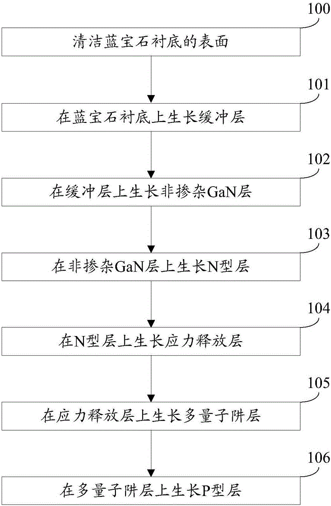
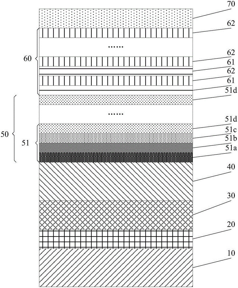
[0026] An embodiment of the present invention provides a method for preparing an epitaxial wafer of a GaN-based light-emitting diode, see figure 1 , the preparation method comprises:
[0027] Step 100: cleaning the surface of the sapphire substrate.
[0028] Specifically, this step 100 may include:
[0029] The sapphire substrate was heated to 1110°C in a Metal-organic Chemical Vapor Deposition (MOCVD) reaction chamber, and the 2 ) atmosphere to anneal the sapphire substrate for 8 to 10 minutes.
[0030] In practical applications, a Si substrate or a SiC substrate may also be used to replace the sapphire substrate.
[0031] Step 101: growing a buffer layer on a sapphire substrate.
[0032] Specifically, this step 101 may include:
[0033] Control the growth temperature to 540°C, and grow a GaN buffer layer with a thickness of 30nm on the sapphire substrate.
[0034] Step 102: growing a non-doped GaN layer on the buffer layer.
[0035] Specifically, this step 102 may inc...
PUM
| Property | Measurement | Unit |
|---|---|---|
| Doping concentration | aaaaa | aaaaa |
Abstract
Description
Claims
Application Information