Transmit-receive Terahertz antenna, manufacturing method therefor and Terahertz measurement system
A measurement system, terahertz technology, applied to antennas, loop antennas, measurement devices, etc., can solve problems affecting practicality, increase system volume, etc., and achieve the effect of great flexibility
- Summary
- Abstract
- Description
- Claims
- Application Information
AI Technical Summary
Problems solved by technology
Method used
Image
Examples
Embodiment 1
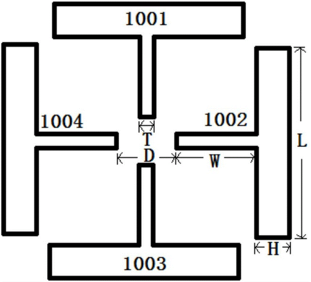
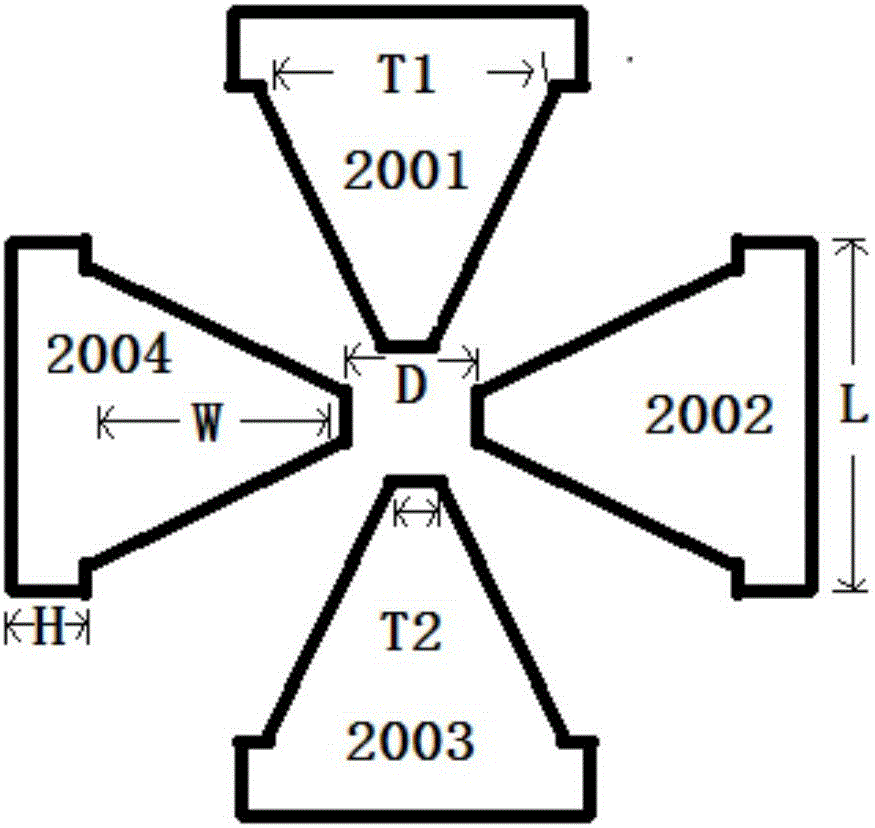
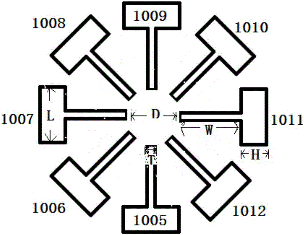
[0056] The terahertz antenna is as image 3 As shown, on a 450 μm thick semi-insulating GaAs substrate 3001, a low-temperature GaAs material layer 3002 with large dark resistance, high carrier mobility, and carrier lifetime in the order of fs is grown, and the material growth of the low-temperature GaAs material layer 3002 The temperature is 250°C, the annealing temperature is 500°C, the annealing time is 10 minutes, and the thickness is 1 μm-2 μm; then, a Ni / Ge / Au alloy or Ti / Pt / Au electrode 3003 with a thickness of 500 nm is deposited by electron beam evaporation, The shape of the electrode 3003 is the same as shown in Figure 1(a), Figure 1(b), Figure 1(c), Figure 1(d) and Figure 1(e), with three, four, eight, twelve The antenna structure of the same electrode is annealed to form ohmic contact with the low-temperature GaAs material layer 3002; finally, SiO with antireflection and insulation protection is grown in the central gap region of the electrode 2 / Si 3 N 4 Insulat...
Embodiment 2
[0063] The terahertz antenna is as image 3 As shown, on an intrinsic InP substrate 3001, an InGaAs:Be / InAlAs multi-quantum well layer material layer 3002 with large dark resistance and high carrier mobility is grown for about 100 cycles, and the thickness of the InAlAs layer is 7- 9nm, the thickness of the InGaAs:Be layer is between 8-14nm, and the total thickness is 1μm-2μm; then use the electron beam evaporation process to deposit a Ni / Ge / Au alloy or Ti / Pt / Au electrode 3003 with a thickness of 500nm, the electrode The shape of 3003 is the same as that shown in Figure 1(a), Figure 1(b), Figure 1(c), Figure 1(d) and Figure 1(e), with three, four, eight and twelve identical The antenna structure of the electrode is annealed to form an ohmic contact with the material layer 3002; finally, SiO with antireflection and insulation protection functions is grown in the gap region of the electrode 2 / Si 3 N 4 Insulation film 3004.
[0064] For the structure of Fig. 1(a), W=450 μm, ...
Embodiment 3
[0070] The antenna structures involved in Embodiments 1 and 2 may be antenna array structures, where the single antenna 2020 may be any multipole antenna structure, and the antenna structures may be consistent or inconsistent. Such as figure 2 As shown, each individual antenna 2020 has the same structure.
[0071] Using the ring-distributed multi-pole terahertz antenna structure, a terahertz spectral measurement system with two different radiation modes, pulse and continuous, can be built. The most important feature of the measurement system is that the transmission and reception of terahertz radiation signals can be realized simultaneously through a circular distributed multipole antenna.
PUM
| Property | Measurement | Unit |
|---|---|---|
| angle | aaaaa | aaaaa |
| angle | aaaaa | aaaaa |
| thickness | aaaaa | aaaaa |
Abstract
Description
Claims
Application Information


