Array substrate, manufacturing method thereof, display panel and manufacturing method thereof

A manufacturing method and array substrate technology, which are applied in the manufacture of semiconductor/solid-state devices, electrical components, and electrical solid-state devices, etc., can solve the problems of large off-state current, affecting the display effect of display devices, and large leakage current of switching transistors.

Active Publication Date: 2016-11-09
BOE TECH GRP CO LTD
View PDF3 Cites 14 Cited by
  • Summary
  • Abstract
  • Description
  • Claims
  • Application Information

AI Technical Summary

Problems solved by technology

The structure of the array substrate used to drive the display device for display, such as figure 1 As shown, it mainly includes: a light-shielding layer 1, a buffer layer 2, an active layer 3, a gate insulating layer 4, an interlayer dielectric layer 5, a gate 6, a source 7 and a drain 8, and a common electrode located on the substrate. 9. Pixel electrode 10; wherein, the active layer is made of polysilicon material, and the light-shielding layer is used to block the influence of external light on the polysilicon material, so as to prevent the active layer from generating photogenerated carriers, thereby affecting the switching characteristics of the switching transistor
However, the switching transistor using polysilicon material as the active layer material has a large off-state current, which causes the switching transistor to have a large leakage current, which makes the switching characteristics of the pixels in the display area unstable, affects the display effect of the display device, and reduces In order to show the yield rate of the product; but its high electron mobility makes it have a high driving ability, so the switching transistor of the active layer is made of polysilicon material, which is suitable for building the driving circuit around the array substrate

Method used


Image

  • Array substrate, manufacturing method thereof, display panel and manufacturing method thereof
  • Array substrate, manufacturing method thereof, display panel and manufacturing method thereof
  • Array substrate, manufacturing method thereof, display panel and manufacturing method thereof

Examples


Embodiment Construction

[0051] The specific implementations of the array substrate, its manufacturing method, display panel and its manufacturing method provided by the embodiments of the present invention will be described in detail below with reference to the accompanying drawings.

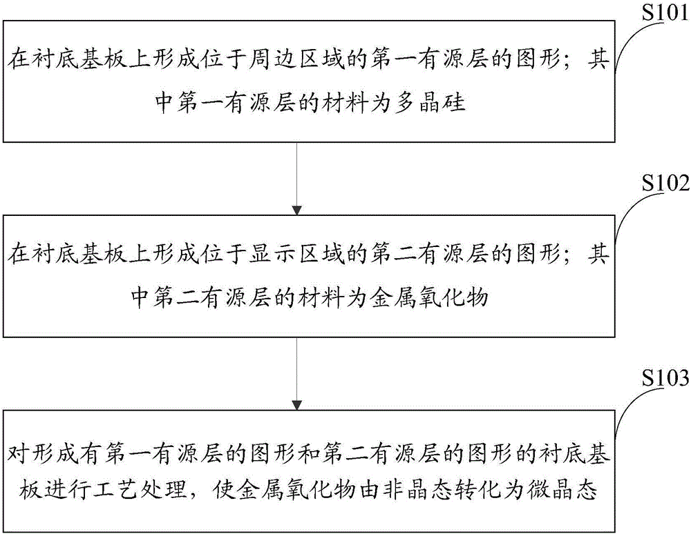
[0052] An embodiment of the present invention provides a method for manufacturing an array substrate, such as figure 2 As shown, can include:

[0053] S101, forming a pattern of a first active layer located in a peripheral region on a base substrate; wherein the material of the first active layer is polysilicon;

[0054] S102, forming a pattern of the second active layer located in the display area on the base substrate; wherein the material of the second active layer is metal oxide;

[0055] S103. Process the base substrate on which the pattern of the first active layer and the pattern of the second active layer are formed, so as to transform the metal oxide from an amorphous state to a microcrystalline state.

[0...


PUM


Abstract

The invention discloses an array substrate, a manufacturing method thereof, a display panel and a manufacturing method thereof. A first active layer manufactured from a metal oxide is used in a display area on the array substrate, so that the off-state current of a formed first switch transistor is relatively low, the metal oxide through fabrication processing can become into a microcrystal state from an amorphous state, and the stability of the first switch transistor is improved; and moreover, a second active layer manufactured from a polycrystalline silicon material is used in a surrounding area on the array substrate, so that a formed second switch transistor has relatively high electron mobility and relatively high drive capability and is applicable to constructing a drive circuit, and the requirement of an integrated drive circuit design in the surrounding area on the array substrate is met. In conclusion, the active layers of the switch transistors manufactured from the metal oxide and the polycrystalline silicon are used in the display area and the surrounding area on the array substrate respectively, so that the structural design of the array substrate is optimized, the display effect of the display product is guaranteed, and the product yield is improved.

Description

technical field [0001] The present invention relates to the field of display technology, in particular to an array substrate, a manufacturing method thereof, a display panel and a manufacturing method thereof. Background technique [0002] Currently, display technology is widely used in displaying televisions, mobile phones, and public information. The structure of the array substrate used to drive the display device for display, such as figure 1 As shown, it mainly includes: a light-shielding layer 1, a buffer layer 2, an active layer 3, a gate insulating layer 4, an interlayer dielectric layer 5, a gate 6, a source 7 and a drain 8, and a common electrode located on the substrate. 9. Pixel electrode 10; wherein, the active layer is made of polysilicon material, and the light-shielding layer is used to block the influence of external light on the polysilicon material, so as to prevent the active layer from generating photogenerated carriers, thereby affecting the switching ...

Claims


Application Information

Patent Timeline
Patent Type & Authority Applications(China)
IPC IPC(8): H01L27/12H01L27/14H01L21/77
CPCH01L21/77H01L27/12H01L27/1222H01L27/1229H01L27/127
Inventor 孙双彭宽军
Owner BOE TECH GRP CO LTD
Why Eureka
Try Eureka