Insulated gate bipolar transistor structure and manufacturing method thereof

A technology of bipolar transistors and insulated gates, applied in transistors, semiconductor/solid-state device manufacturing, semiconductor devices, etc., can solve difficult problems and achieve low on-state voltage drop

Active Publication Date: 2016-11-09
宁波吉赛半导体有限公司
View PDF5 Cites 2 Cited by
  • Summary
  • Abstract
  • Description
  • Claims
  • Application Information

AI Technical Summary

Problems solved by technology

However, it is practically very difficult to fabric

Method used


Image

  • Insulated gate bipolar transistor structure and manufacturing method thereof
  • Insulated gate bipolar transistor structure and manufacturing method thereof
  • Insulated gate bipolar transistor structure and manufacturing method thereof

Examples


Embodiment Construction

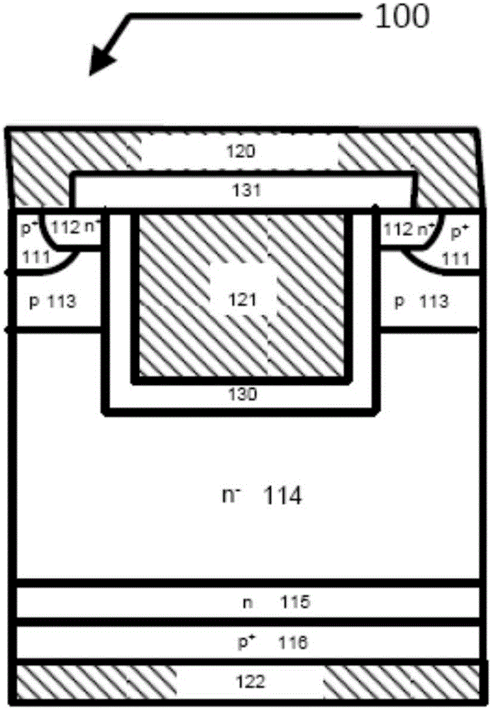
[0088] The invention will be described using n-channel devices, but it will be understood in the following description that the invention is equally applicable to p-channel devices. In the specification of the present invention, the heavily doped n-type region is marked as n + , and the heavily doped p-type region is labeled p + , in silicon, unless otherwise stated, heavily doped regions typically have 19 cm -3 with 1×10 21 cm -3 Doping concentration between. In the specification of the present invention, the lightly doped n-type region is marked as n - , and the lightly doped p-type region is labeled p - , in silicon, unless otherwise stated, lightly doped regions typically have 13 cm -3 with 1×10 17 cm -3 Doping concentration between.

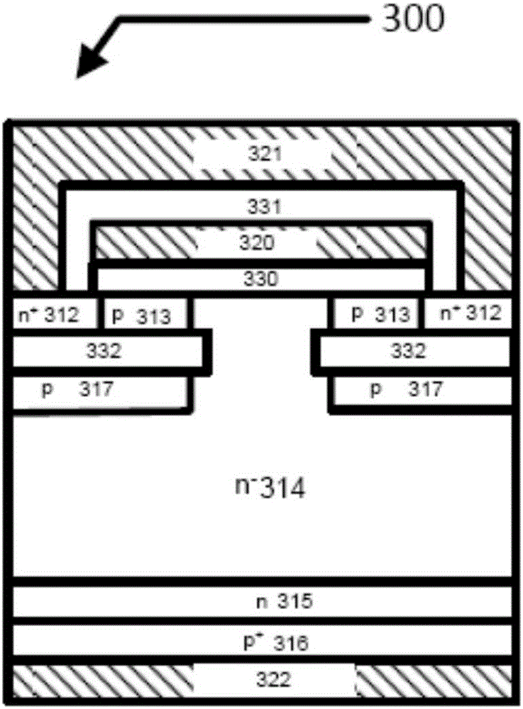
[0089] image 3 is a cross-sectional view of the invention implemented in IGBT device 300, Figure 4 is a top view of the same device 300 . Device 300 includes: a collector (322) at the bottom; a p + collector area (316); loca...


PUM

PropertyMeasurementUnit
Doping concentrationaaaaaaaaaa
Lengthaaaaaaaaaa

Abstract

The invention provides an insulated gate bipolar transistor (IGBT) structure and a manufacturing method thereof. The structure is a planar IGBT structure; and the insulated gate bipolar transistor (IGBT) structure is characterized by comprising an ultra-thin channel and a buried oxide located under the channel. By the structure, a theoretic lowest on-state voltage drop can be provided.

Description

technical field [0001] The present invention relates generally to the structure and fabrication process of power semiconductor devices, and in particular to IGBTs. Background of the invention [0002] Insulated gate bipolar transistors (IGBTs) have been widely used in high voltage power electronic systems, such as variable frequency drives and inverters, where it is desirable to have low power losses within the device. The conduction loss of IGBT is the main component of power loss, and the conduction loss can be characterized by the on-state voltage drop of the device. It is therefore an object of the present invention to provide an IGBT with the theoretically lowest on-state voltage drop. [0003] current technology [0004] figure 1 A cross section of a prior art IGBT device 100 is shown. Device 100 is a MOS controlled PNP bipolar junction transistor. MOS channel by n + Emitter region (112), p-type base region (113), n - A drift region (114), a gate dielectric (130...

Claims


Application Information

Patent Timeline
IPC IPC(8): H01L29/739H01L29/06H01L21/331
CPCH01L29/0688H01L29/66333H01L29/7398
Inventor 周贤达黄嘉杰单建安
Owner 宁波吉赛半导体有限公司
Why Eureka
Try Eureka