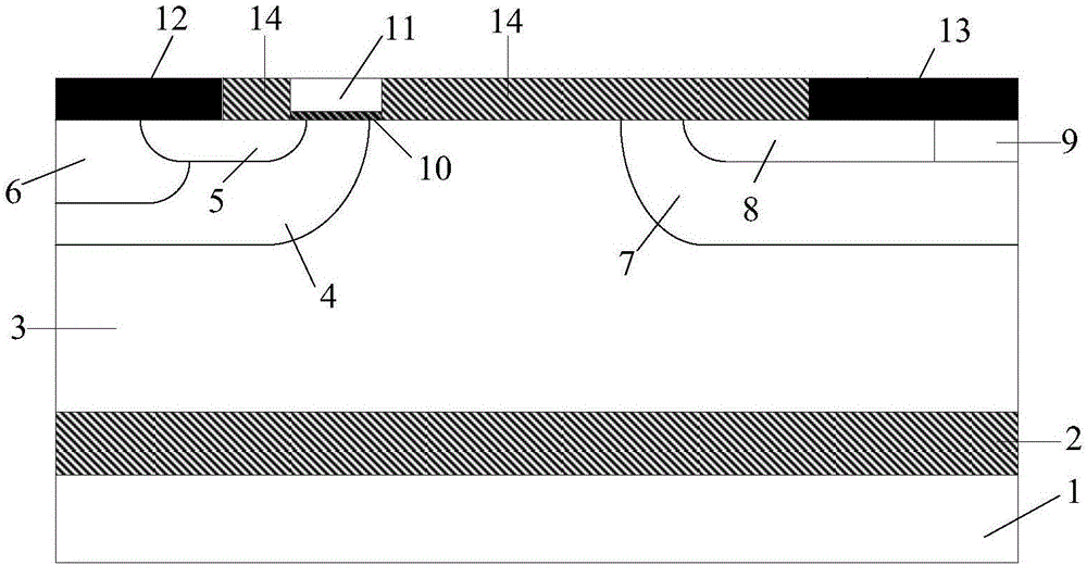
Two-channel RC-LIGBT device and manufacturing method thereof
A dual-channel, device technology, applied in semiconductor/solid-state device manufacturing, semiconductor devices, electrical components, etc., can solve the problems that affect the stability and reliability of LIGBT devices, the PN junction cannot be opened normally, and the PN junction conduction voltage drop increases and other issues, to achieve the effect of improving stability and reliability, low conduction voltage drop, and strong freewheeling ability
- Summary
- Abstract
- Description
- Claims
- Application Information
AI Technical Summary
Problems solved by technology
Method used
Image
Examples
Embodiment 1
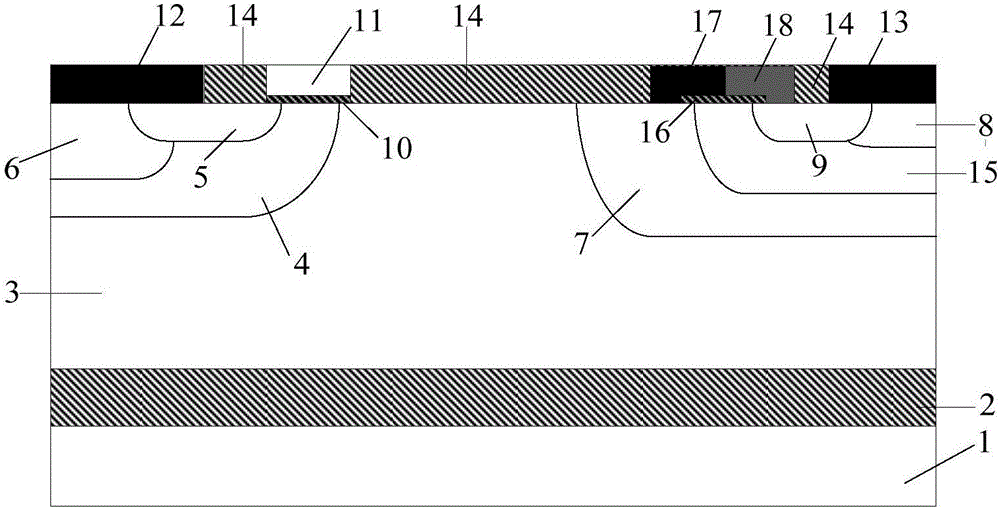
[0035] This embodiment provides a dual-channel RC-LIGBT device with a voltage level of 400V, and its cell structure is as follows figure 2 As shown, it includes a substrate 1, a silicon oxide dielectric layer 2 on the substrate 1, an N-type drift region 3 on the silicon oxide dielectric layer 2, an emitter structure on the N-type drift region 3, a gate structure, The collector structure and the first dielectric layer 14; the emitter structure is composed of a P-type base region 4, an N+ source region 5, a P+ contact region 6 and a metal emitter 12, wherein the P-type base region 4 is set on the N-type drift In region 3 and located on the left side of its top, P+ contact region 6 and N+ source region 5 are independently arranged in P-type base region 4, and the front surfaces of P+ contact region 6 and N+ source region 5 are both in phase with metal emitter 12 Contact; the gate structure is located on the side of the emitter structure and consists of a gate dielectric 10 and a...
Embodiment 2
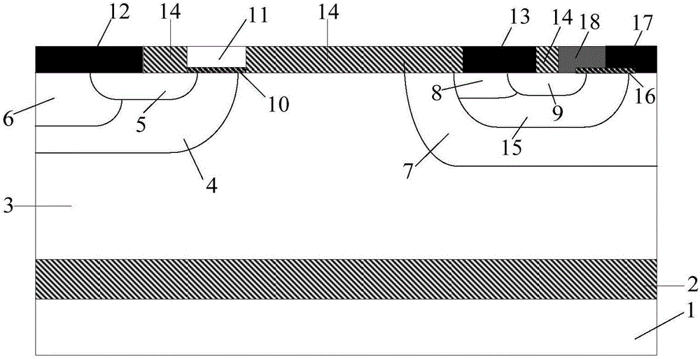
[0038] This embodiment provides a dual-channel RC-LIGBT device with a voltage level of 400V, and its cell structure is as follows image 3As shown, it includes a substrate 1, a silicon oxide dielectric layer 2 on the substrate 1, an N-type drift region 3 on the silicon oxide dielectric layer 2, an emitter structure on the N-type drift region 3, a gate structure, A collector structure and a dielectric layer 14; the emitter structure is composed of a P-type base region 4, an N+ source region 5, a P+ contact region 6 and a metal emitter 12, wherein the P-type base region 4 is arranged in the N-type drift region 3 and located on the left side of its top, the P+ contact region 6 and the N+ source region 5 are independently arranged in the P-type base region 4, and the front surfaces of the P+ contact region 6 and the N+ source region 5 are in contact with the metal emitter 12; The gate structure is located on the right side of the emitter structure and is composed of a gate dielect...
PUM
 Abstract
Description
Claims
Application Information


