
Microstrip array antenna loaded with graphene decoupling network
A technology of decoupling network and microstrip array, applied in the directions of antenna, antenna coupling, antenna array, etc., can solve the problems of large size of microstrip array antenna and poor unit isolation, and achieve the effect of improving isolation
- Summary
- Abstract
- Description
- Claims
- Application Information
AI Technical Summary
Problems solved by technology
Method used
Image

Examples
Embodiment Construction
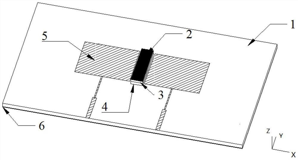
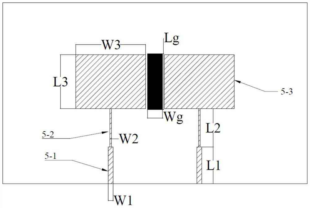
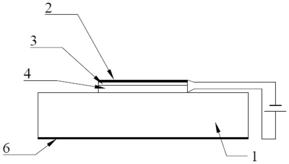
[0023] A microstrip array antenna loaded with a graphene-2 decoupling network, such as figure 1 with 2 As shown, it consists of a dielectric board 1 , a metal floor 6 , and more than two independent antenna array units 5 . The metal floor 6 and the antenna array unit 5 can be located on the same side surface of the dielectric board 1 , or can be located on different side surfaces of the dielectric board 1 . In a preferred embodiment of the present invention, the metal floor 6 is located on the lower surface of the dielectric board 1 , and all the antenna array units 5 are located on the upper surface of the dielectric board 1 .
[0024] The dielectric board 1 is used as the dielectric board 1 of the array antenna, with a length×width×thickness of 160mm×95mm×0.8mm, a relative permittivity of 4.4, and a loss tangent of 0.02. The distance between the edge of the dielectric plate 1 and the edge of the radiation patch 5-3 is slightly greater than a quarter of a wavelength, so t...
PUM
| Property | Measurement | Unit |
|---|---|---|
| thickness | aaaaa | aaaaa |
| relative permittivity | aaaaa | aaaaa |
| relative permittivity | aaaaa | aaaaa |
Abstract
Description
Claims
Application Information