Pixel circuit and display device

A pixel circuit and capacitor technology, applied in the field of display devices, can solve the problems of not being suitable for displays, long set-up time, affecting aperture ratio and yield, etc., and achieve the effect of solving different threshold voltages and reducing correlation

Active Publication Date: 2016-11-16
PEKING UNIV SHENZHEN GRADUATE SCHOOL
View PDF4 Cites 9 Cited by
  • Summary
  • Abstract
  • Description
  • Claims
  • Application Information

AI Technical Summary

Problems solved by technology

Current programming has a good compensation effect, but it takes a long time to set up under low current, so it is not suitable for manufacturing medium and large-sized displays; although the voltage

Method used


Image

  • Pixel circuit and display device
  • Pixel circuit and display device
  • Pixel circuit and display device

Examples


Embodiment 1

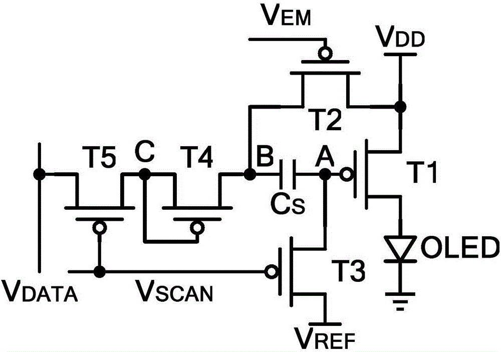
[0040] Please refer to figure 2 , the pixel circuit in this embodiment includes a first transistor T1, a second transistor T2, a third transistor T3, a fourth transistor T4, a fifth transistor T5, a first capacitor C S and the light emitting device OLED; in this embodiment, the first transistor T1 and the fourth transistor T4 are both P-type transistors, and the second transistor T2, the third transistor T3, and the fifth transistor T5 are also P-type transistors.

[0041] The first transistor T1 and the light emitting device OLED are serially connected between the power supply voltage and the ground, and the first transistor T1 is used as a driving transistor to provide a driving current for the light emitting device OLED; the gate of the first transistor T1 is connected to the second capacitor of the first capacitor CS One electrode, the first electrode of the first transistor T1 is connected to the supply voltage line V DD , the second electrode of the first transistor T1...

Embodiment 2

[0060] Such as Figure 5 As shown, the main difference from the first embodiment is that the second transistor T2 is an N-type transistor, and the third transistor and the fifth transistor are P-type transistors. In this way, the light emission control signal and the scan control signal that the second transistor T2 responds to are the same control signal, and the control electrode of the second transistor T2 can be directly connected to the scan control signal line VSCAN, which can reduce a set of scan control signal generation circuits and simplify The peripheral circuit makes the control signal of the pixel circuit only need one scan line, and is directly compatible with the gate drive circuit of the display device. Devices whose connection relationship does not change in the circuit will not be described here.

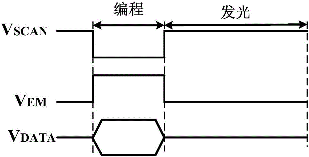
[0061] Please refer to Figure 6 , the driving process is the same as that of Embodiment 1, and also includes a programming phase and a light emitting phase. In...

Embodiment 3

[0064] In the above embodiment, in the branch formed by the third transistor T3, the first capacitor Cs and the fifth transistor T5, the fourth transistor T4 is connected between the second electrode of the fifth transistor T5 and the second terminal of the first capacitor Cs Between, this embodiment is different from the foregoing embodiments in that the fourth transistor is connected between the first electrode of the third transistor and the first terminal of the first capacitor.

[0065] Please refer to Figure 8 , the pixel circuit in this embodiment includes a first transistor T1, a second transistor T2, a third transistor T3, a fourth transistor T4, a fifth transistor T5, a first capacitor C S and the light emitting device OLED; in this embodiment, the first transistor T1 and the fourth transistor T4 are both P-type transistors, and the second transistor T2, the third transistor T3, and the fifth transistor T5 are also P-type transistors.

[0066] The first transistor T1...


PUM


Abstract

The invention provides a pixel circuit and a display device. The pixel circuit comprises a first transistor, a second transistor, a third transistor, a fourth transistor, a fifth transistor, a first capacitor and a light emitting unit. The first end of the first capacitor is connected to a control electrode of the first transistor, and a second end is connected to a power supply voltage line via the second transistor. The third transistor is connected between the first capacitor and a reference level signal line, with a control electrode being connected to a scanning control signal line. The fifth transistor is connected between a data signal line and the first capacitor, with a control electrode being connected to the scanning control signal line. A grid electrode of the fourth transistor is connected to its own first electrode. The fourth transistor is connected between the third transistor and the first capacitor, or the fourth transistor is connected between the fifth transistor and the first capacitor. The invention can solve the problem of display unevenness which may be caused due to different threshold voltages of drive transistors on a display panel and IR-Drop on a VDD line.

Description

technical field [0001] The present application relates to the field of display devices, in particular to a display device and a pixel circuit thereof. Background technique [0002] Organic Light-Emitting Diode (OLED: Organic Light-Emitting Diode) display has been widely studied in recent years due to its advantages of high brightness, high luminous efficiency, wide viewing angle, low power consumption, and low manufacturing cost, and has been rapidly applied to a new generation of displays. device. OLED displays can be divided into two types: PMOLED (Passive Matrix OLED: Passive Matrix OLED) and AMOLED (Active Matrix OLED: Active Matrix OLED) according to the pixel driving method. Although PMOLED has low manufacturing cost, it has crosstalk and requires a large driving current, so it has disadvantages such as short service life and high power consumption, and cannot meet the display requirements of large area and high resolution. In contrast, AMOLED avoids problems such as...

Claims


Application Information

Patent Timeline
IPC IPC(8): G09G3/3225
CPCG09G3/3225
Inventor 张盛东王翠翠孟雪
Owner PEKING UNIV SHENZHEN GRADUATE SCHOOL
Why Eureka
Try Eureka