Two-way integrated embedded chip rerouting POP packaging structure and manufacturing method thereof

A packaging structure and rewiring technology, applied in semiconductor/solid-state device manufacturing, electrical components, electric solid-state devices, etc., can solve the problem of low precision of laser drilling and electroplating blind hole process, easily deformable thickness of substrate, unfavorable packaging integration degree, etc. problems, to achieve better product performance, better electrical and heat dissipation performance, and high integration

Inactive Publication Date: 2016-11-16
江阴芯智联电子科技有限公司
View PDF5 Cites 12 Cited by
  • Summary
  • Abstract
  • Description
  • Claims
  • Application Information

AI Technical Summary

Problems solved by technology

The current traditional three-dimensional packaging structure such as figure 1 As shown, the production method is to embed passive and active components on one side of the substrate, press or coat insulating materials, and use laser drilling and electroplating blind hole technology to lead the underlying functions to the second connection layer and then mak...

Method used


Image

  • Two-way integrated embedded chip rerouting POP packaging structure and manufacturing method thereof
  • Two-way integrated embedded chip rerouting POP packaging structure and manufacturing method thereof
  • Two-way integrated embedded chip rerouting POP packaging structure and manufacturing method thereof

Examples


Embodiment Construction

[0050] The present invention will be further described in detail below in conjunction with the accompanying drawings and embodiments.

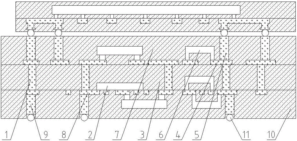
[0051] like figure 2 As shown, a bidirectional integrated embedded chip redistribution POP package structure in this embodiment includes a first package body and a second package body, the first package body includes a second circuit layer 8, and the first package body includes a second circuit layer 8. The front side of the second circuit layer 8 is provided with a first connecting copper column 1 and a first component 2, and the periphery of the first connecting copper column 1 and the first component 2 is encapsulated with a first insulating material 3, and the first insulating material 3. A first circuit layer 4 is provided on the front side, and a second connection copper column 5 and a second component 6 are provided on the front side of the first circuit layer 4, and the outer periphery of the second connection copper column 5 and the ...


PUM


Abstract

The invention relates to a two-way integrated embedded chip rerouting POP packaging structure and a manufacturing method thereof. The structure comprises a first packaging body and a second packaging body, wherein the first packaging body comprises a second circuit layer (8); the front surface of the second circuit layer (8) is provided with first connecting copper cylinders (1) and first components (2); a first insulating material (3) packages the outside of the first connecting copper cylinders (1) and first components (2); the front surface of the first insulating layer (3) is provided with a first circuit layer (4); the front surface of the first circuit layer (4) is provided with second connecting copper cylinders (5) and second components (6); a second insulating material (7) packages the outside of the second connecting copper cylinders (5) and the second components (6); the back surface of the second circuit layer (8) is provided with third connecting copper cylinders (9); and the third connecting copper cylinders (9) are provided with metal balls (11). The two-way integrated embedded chip rerouting POP packaging structure can be embedded in multi-layer and two-way manners; the placement number of passive devices is larger; the substrate space is effectively saved; and the integration level of a packaging technology is improved.

Description

technical field [0001] The invention relates to a bidirectional integrated embedded chip rewiring POP packaging structure and a manufacturing method thereof, belonging to the technical field of semiconductor packaging. Background technique [0002] With the development of electronic devices towards high functionality and miniaturization, the proportion of passive devices in electronic systems is also increasing. At present, passive devices are mainly surface-mounted, which not only occupies a large amount of space on the surface of the substrate, but also has a large number of solder joints on the surface and a long interconnection length, which greatly reduces the electrical performance and reliability of the system. In order to save the surface space of the circuit board / substrate and provide thinner, better performance, and more reliable electronic systems, surface mount passive devices are transformed into embeddable passive devices, and all active components are buried ...

Claims


Application Information

Patent Timeline
IPC IPC(8): H01L23/14H01L23/498H01L21/48
CPCH01L2224/16225H01L2924/15311H01L2924/19105H01L23/142H01L21/4853H01L23/49811H01L23/49838
Inventor 王新潮陈灵芝张凯郁科锋
Owner 江阴芯智联电子科技有限公司
Why Eureka
Try Eureka