Laser annealing device and annealing method thereof

A laser annealing and annealing technology, applied in electrical components, semiconductor/solid-state device manufacturing, circuits, etc., can solve the problems of reducing scanning uniformity, unable to adjust the relative position and spot size, affecting the annealing performance of silicon wafers, and improving the annealing performance. Effects of performance and ductility

Active Publication Date: 2016-11-23
SHANGHAI MICRO ELECTRONICS EQUIP (GRP) CO LTD
View PDF9 Cites 6 Cited by
  • Summary
  • Abstract
  • Description
  • Claims
  • Application Information

AI Technical Summary

Problems solved by technology

However, using this method will result in a change in the incident angle and reduce the uniformity of the scan
[0004] Later, a semiconductor manufacturing method and device was proposed, using two different laser beams for deep annealing, at least one of which is a continuous laser beam, and different annealing temperatures are controlled according to the depth of the silicon wa

Method used


Image

  • Laser annealing device and annealing method thereof
  • Laser annealing device and annealing method thereof
  • Laser annealing device and annealing method thereof

Examples


Embodiment Construction

[0041] The present invention is described in detail below in conjunction with accompanying drawing:

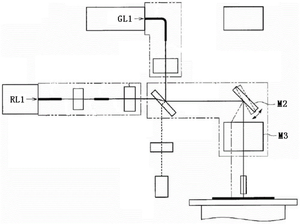
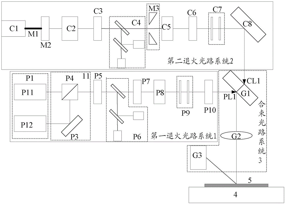
[0042] Such as figure 2 As shown, the present invention provides a laser annealing device, including a first annealing optical path system 1, a second annealing optical path system 2 and a beam combining optical path system 3, wherein the first annealing optical path system 1 includes a visible laser light source P1, and a visible laser light source P1 The corresponding visible laser light path system and the first energy monitoring unit P6; the second annealing light path system 2 includes a near-infrared laser light source C1, a near-infrared laser light path system corresponding to the near-infrared laser light source C1, a second energy monitoring unit C4 and an energy adjustment Unit M3; the near-infrared laser optical path system includes a near-infrared laser light source position adjustment unit M2; the beam combining optical path system 3 is arranged after the first ...


PUM

PropertyMeasurementUnit
Wavelengthaaaaaaaaaa

Abstract

The invention discloses a laser annealing device and an annealing method thereof. The annealing device comprises a first annealing optical path system, a second annealing optical path system and a beam combining optical path system; the first annealing optical path system includes a visible laser light source, a visible laser optical path system corresponding to the visible laser light source, and a first energy monitoring unit; the second annealing optical path system includes a near infrared laser light source, a near infrared laser optical path system corresponding to the near infrared laser light source, a second energy monitoring unit and an energy adjustment unit; the near infrared laser optical path system includes a near infrared laser light source position adjustment unit; and the beam combining optical path system is arranged behind the visible laser optical path system and the near infrared laser optical path system and before a workpiece stage. According to the laser annealing device and the annealing method thereof of the invention, the relative sizes and positions of two annealing light spots are adjusted through the energy adjustment unit and the near infrared laser light source position adjustment unit, so that the dwell time and annealing temperature of annealing are controlled, and annealing requirements of different positions of a wafer can be satisfied, and the annealing performance of a system can be improved.

Description

technical field [0001] The invention relates to the technical field of laser annealing, in particular to a laser annealing device and an annealing method thereof. Background technique [0002] In the manufacture of semiconductor devices, when ion implantation is performed in a predetermined area on the back of a silicon substrate, P ions are usually implanted in the deep layer and B ions are implanted in the shallow layer, and the solubility of B ions is higher than that of P ions in the deep layer. Therefore, the use of this ion implantation method is likely to damage the crystallinity of the surface of the silicon substrate, making the arrangement of ions disorderly. In response to the above problems, laser annealing is usually used for semiconductor films formed on insulating substrates such as glass to achieve crystallization or increase crystallinity, and the result of laser annealing is to convert amorphous materials into polycrystalline or In the single crystal state...

Claims


Application Information

Patent Timeline
IPC IPC(8): H01L21/268
Inventor 王成才兰艳平徐建旭
Owner SHANGHAI MICRO ELECTRONICS EQUIP (GRP) CO LTD
Why Eureka
Try Eureka