Device for manufacturing integrated thin film solar cell

A solar cell and thin film technology, applied in circuits, photovoltaic power generation, electrical components, etc., can solve the problems of expensive integrated transparent thin film solar cells and rising manufacturing costs of integrated thin film solar cells, and achieve the effect of low manufacturing

Inactive Publication Date: 2016-11-23
KOREA ADVANCED INST OF SCI & TECH
View PDF20 Cites 2 Cited by
  • Summary
  • Abstract
  • Description
  • Claims
  • Application Information

AI Technical Summary

Problems solved by technology

Therefore, the manufacturing cost of integrated thin-film solar cells rises
[0012] In addition, in the manufacture of integrated transparent thin film solar cells using laser patterning technology, integrated transparent thin film solar cells become more expensive

Method used


Image

  • Device for manufacturing integrated thin film solar cell
  • Device for manufacturing integrated thin film solar cell
  • Device for manufacturing integrated thin film solar cell

Examples


Embodiment Construction

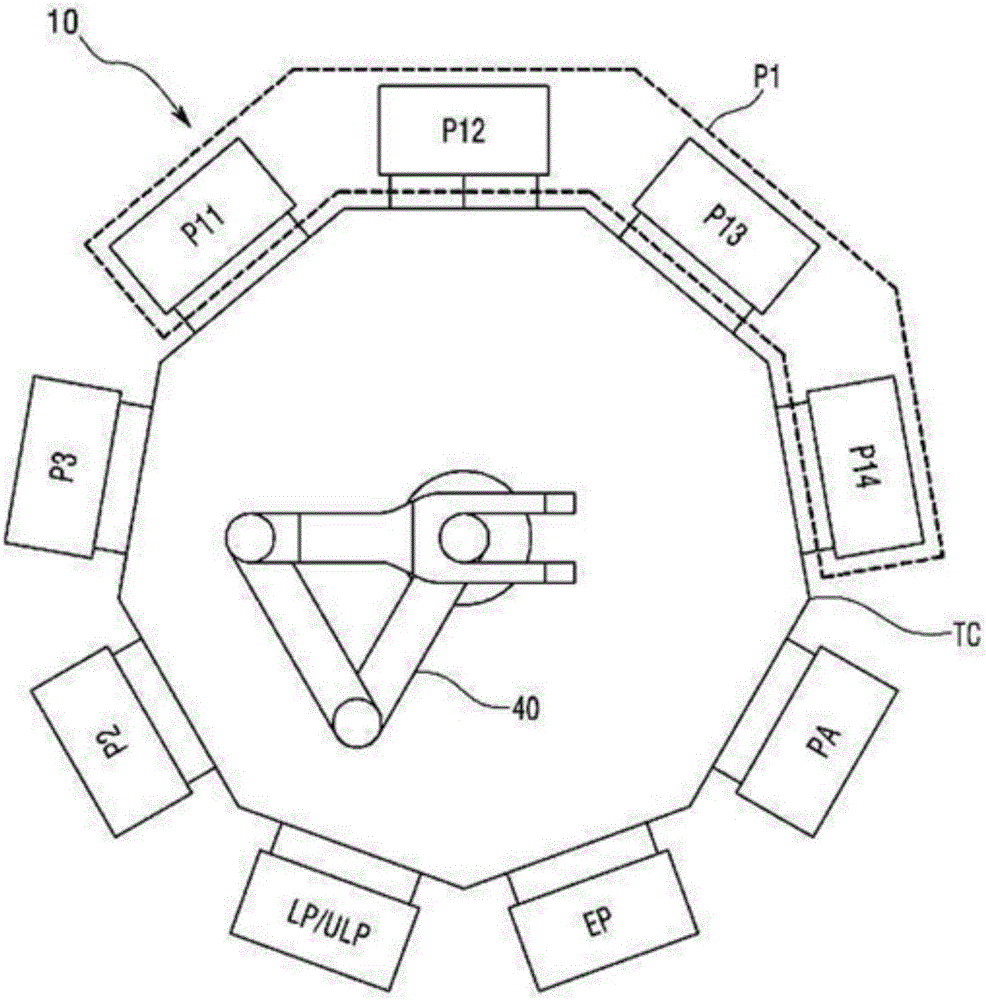
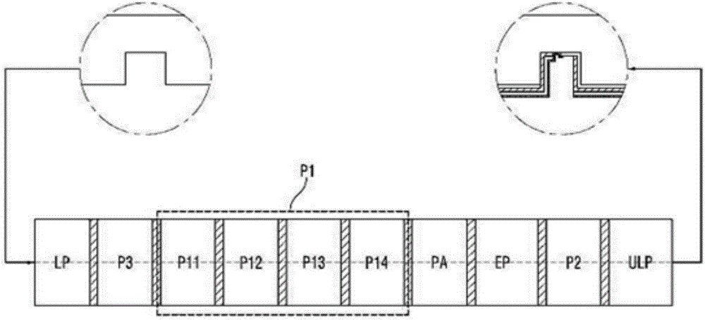
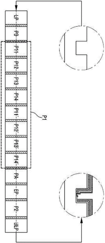
[0036] The device for manufacturing an integrated thin-film solar cell according to an embodiment of the present invention can be applied to the integration of all dry-type thin-film solar cells. However, for the sake of convenience, the embodiments of the present invention will be described in detail below with reference to the accompanying drawings taking an amorphous silicon-based thin-film silicon solar cell as an example. The amorphous silicon-based thin-film silicon solar cell has the most complicated manufacturing process, including photovoltaic Etching of the converter. However, the provided drawings are only for easier description of the present invention. It will be easily understood by those skilled in the art that the spirit and scope of the present invention are not limited to the scope of the accompanying drawings.

[0037] The apparatus for manufacturing an integrated thin film solar cell according to an embodiment of the present invention includes a second con...


PUM


Abstract

A device for manufacturing an integrated thin film solar cell, according to one embodiment of the present invention, is a device for manufacturing an integrated thin film solar cell in which a plurality of unit cells are electrically connected in series in a vacuum state, and the manufacturing device comprises: a photoelectric conversion unit-forming process chamber which forms a photoelectric conversion unit by emitting a photoelectric conversion material onto a substrate having a first conductive layer, which is formed from one base line inside each of a plurality of trenches formed on the substrate to areas such as a bottom surface of each of the trenches, one side surface connected to the bottom surface, and a protruding surface of the substrate connected to the one side surface; and a second conductive layer-forming process chamber which forms a second conductive layer from another base line inside each of the trenches to areas such as the bottom surface of each of the trenches, the other side surface connected to the bottom surface, and a protruding surface of the substrate connected to the other side surface, wherein the photoelectric conversion unit-forming process chamber and the second conductive layer-forming process chamber are capable of performing each of the processes in a vacuum state.

Description

technical field [0001] The present invention relates to a device for the manufacture of integrated thin film solar cells. Background technique [0002] Generally, a solar cell is formed by using a junction consisting of a p-type semiconductor and an n-type semiconductor (i.e., a semiconductor p-n junction), a junction consisting of a metal and a semiconductor (i.e., a metal / semiconductor (MS) junction (so-called Schottky junction)) , or a device that converts sunlight energy into electricity by the photovoltaic effect caused by a metal / insulator / semiconductor (MIS) junction. [0003] Solar cells are mainly classified into silicon-based solar cells, compound-based solar cells, and organic-based solar cells according to materials used for the solar cells. According to the semiconductor phase, silicon solar cells are divided into single crystal silicon (sc-Si) solar cells, polycrystalline silicon (pc-Si) solar cells, microcrystalline silicon (μc-Si:H) solar cells and amorphous...

Claims


Application Information

Patent Timeline
Patent Type & Authority Applications(China)
IPC IPC(8): H01L31/18H01L31/0445
CPCH01L31/046H01L31/0465Y02E10/50H01L31/18H01L31/0463H01L31/0445
Inventor 林宏树全振完洪玧昊
Owner KOREA ADVANCED INST OF SCI & TECH
Why Eureka
Try Eureka