

Light-emitting diode structure and manufacturing method thereof
A technology of light-emitting diodes and manufacturing methods, applied to electrical components, circuits, semiconductor devices, etc., to achieve the effects of increasing the light-emitting area, improving the efficiency of light extraction, and the best light-taking effect
- Summary
- Abstract
- Description
- Claims
- Application Information
AI Technical Summary
Problems solved by technology
Method used
Image

Examples
Embodiment 1
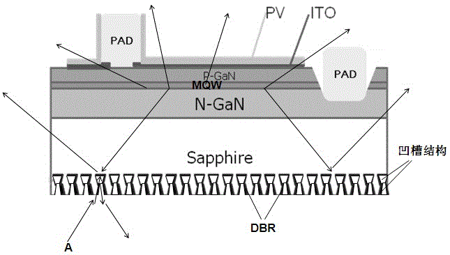
[0032] like figure 1 As shown, a positive light-emitting diode structure includes a substrate, a first semiconductor layer (N-type layer), a second semiconductor layer (P-type layer) and a quantum The light-emitting epitaxial layer composed of the well layer (MQW), the distributed Bragg reflection layer (DBR) on the back of the substrate, the current spreading layer on the P-type layer, the P electrode (PAD) on the current spreading layer and the N-type layer The N electrode (PAD) on the upper surface, and the insulating protective layer (PV), where the back of the substrate has a series of hourglass-shaped groove structures that are periodically and regularly distributed, and the distributed Bragg reflection layer (DBR) fills the groove structure inner wall.
[0033] In this embodiment, the substrate is preferably sapphire, and the above-mentioned light-emitting epitaxial layer can be bonded to the heat-dissipating substrate on the sapphire by using metal organic compound ch...
Embodiment 2
[0039] like Figure 2~6 As shown, this embodiment provides a method for preparing a light-emitting diode structure, the process steps of which include:
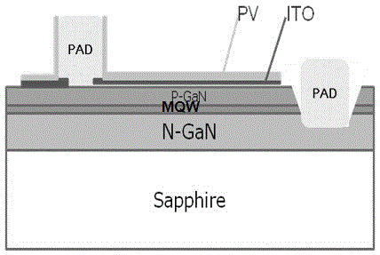
[0040] like figure 2 As shown, a substrate is provided, preferably sapphire (Sapphire), and a light-emitting epitaxial layer is formed on the sapphire (Sapphire) by metal organic compound chemical vapor deposition (MOCVD). The light-emitting epitaxial layer material is a GaN-based compound, including an N-type layer (N-GaN layer), a light-emitting layer (MQW) and a P-type layer (P-GaN layer) from bottom to top. Use ICP process to etch from part of the P-GaN layer to expose part of the N-GaN layer) surface, form an ITO current spreading layer on the P-GaN layer of the light-emitting epitaxial layer, and then respectively on the ITO current spreading layer and the N-GaN layer P-type PADs and N-type PADs are fabricated to realize electrical coupling between P-type and N-type PADs and the light-emitting epitaxial layer. Final...
Embodiment 3
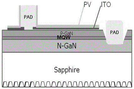
[0045] like Figure 7 As shown, the difference from Example 1 is that the DBR layer in Example 1 is filled in the hourglass-shaped groove structure but not completely, while the DBR layer in this embodiment is filled in the hourglass-shaped groove structure. Since the distributed Bragg reflection layer (DBR) has a more obvious reflection effect on light incident at a small angle, some light incident at a large angle will still pass through the DBR layer. Set the crystal-bonding silver glue (not shown in the figure) at the bottom, so that the light that penetrates the DBR layer (such as figure 1 Medium light A) will be reflected to the DBR layer in the hourglass-shaped groove structure through the crystal-bonding silver glue, and may need to be reflected several times on the inner wall of the groove structure before exiting; when this embodiment is used to make a package, it will penetrate the DBR layer light (such as Figure 7 The middle light B) will be reflected by the cry...
PUM
 Abstract
Description
Claims
Application Information