Eureka AIR delivers breakthrough ideas for toughest innovation challenges, trusted by R&D personnel around the world.

Method for manufacturing a polycrystalline silicon ingot

A polycrystalline silicon ingot and a technology for a manufacturing method are applied in the field of silicon ingot manufacturing, and can solve problems such as the inability to effectively reduce the oxygen impurity concentration of the polycrystalline silicon ingot.

Inactive Publication Date: 2016-12-07
AUO CRYSTAL
View PDF6 Cites 0 Cited by
  • Summary
  • Abstract
  • Description
  • Claims
  • Application Information

AI Technical Summary

Problems solved by technology

However, it has been proved by experiments that oxygen will still diffuse through the silicon nitride layer into the silicon melt, and the silicon nitride layer cannot effectively reduce the oxygen impurity concentration in the polysilicon ingot.

Method used


Image

  • Method for manufacturing a polycrystalline silicon ingot
  • Method for manufacturing a polycrystalline silicon ingot
  • Method for manufacturing a polycrystalline silicon ingot

Examples


Embodiment Construction

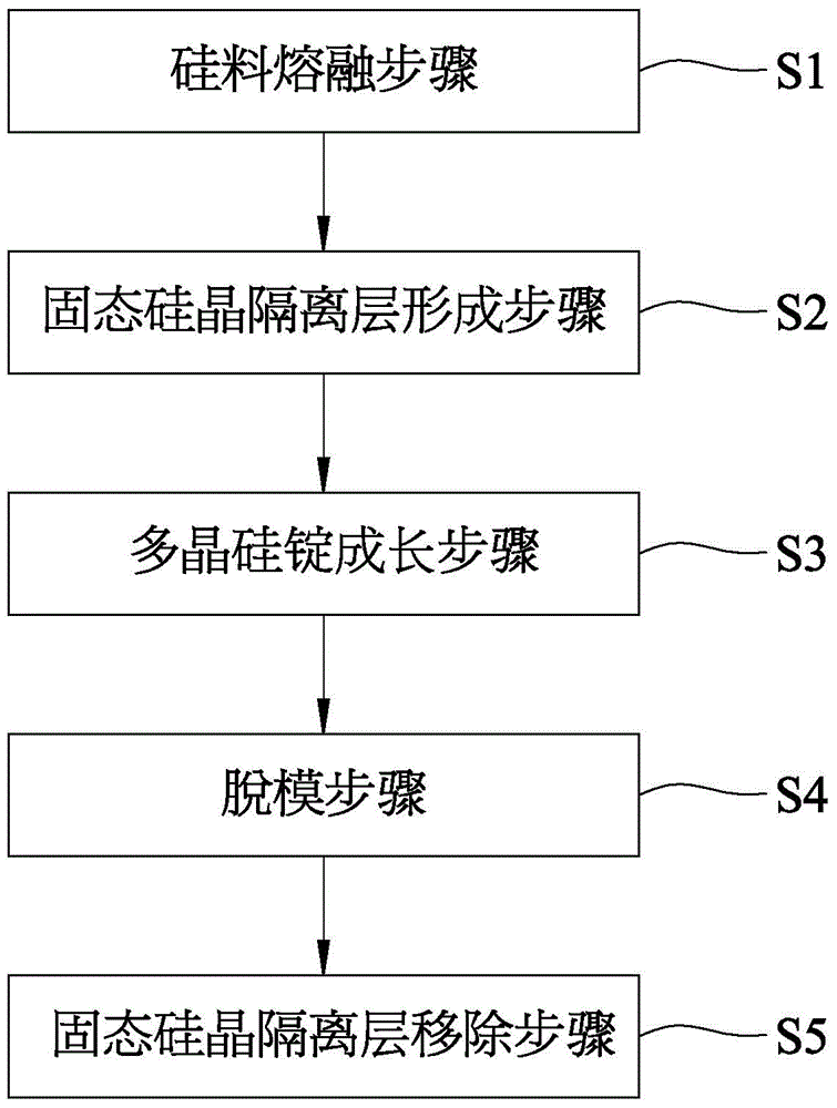
[0028] see figure 1 , an embodiment of the polysilicon manufacturing method of the present invention includes the following steps: a silicon material melting step S1, a solid silicon crystal isolation layer forming step S2, a polycrystalline silicon ingot growing step S3, a demolding step S4, and a solid silicon crystal The isolation layer is removed in step S5.

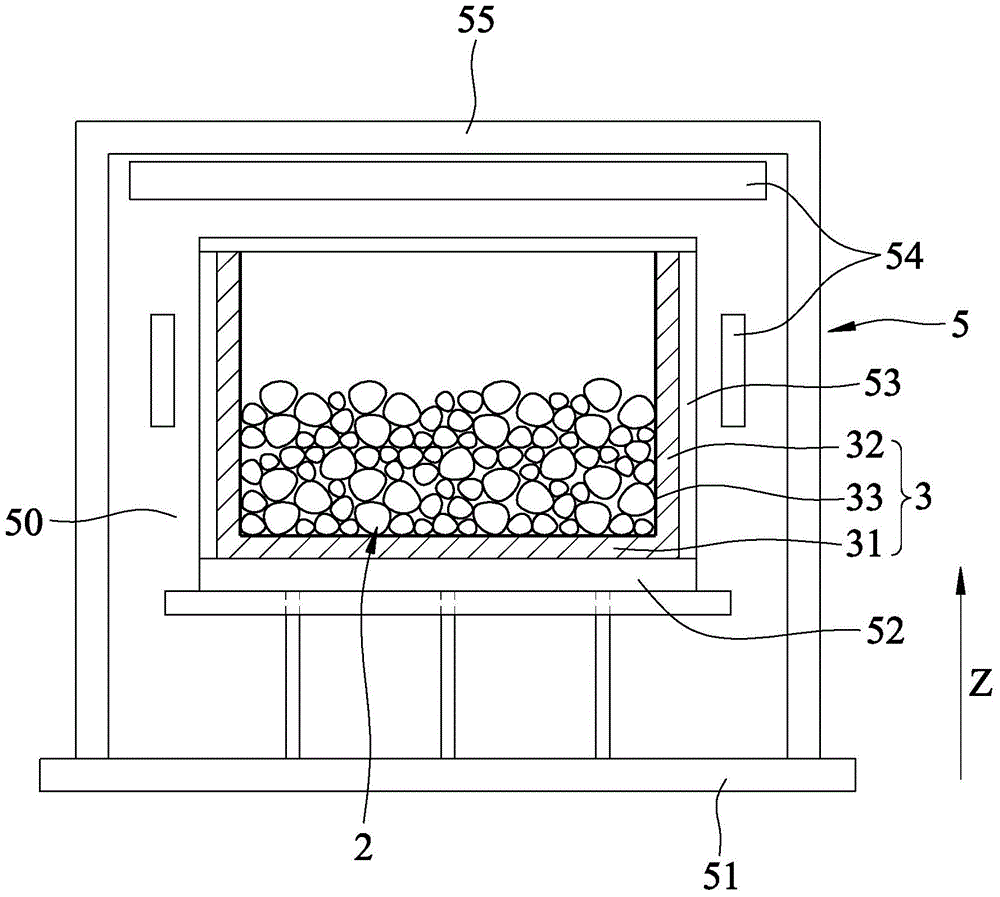
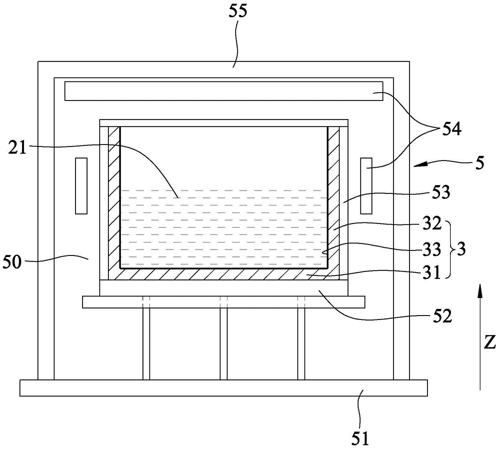
[0029] First, perform the silicon material melting step S1 (see also figure 2 ), a release layer 33 containing a silicon material 2 and having a bottom wall 31, a surrounding wall 32 surrounding the bottom wall 31 and an inner surface formed on both the bottom wall 31 and the surrounding wall 32 The crucible 3 is set in a thermal field 50, so that the silicon material 2 in the crucible 3 is heated by the thermal field 50 to be melted into a silicon molten soup 21 (such as image 3 shown).

[0030] Preferably, the release layer 33 is made of silicon nitride material. The crystal growth furnace system 5 includes a...


PUM


Abstract

A method for manufacturing a polycrystalline silicon ingot includes steps of: A) putting a crucible loaded with a silicon material and having a base and a wall around the base in a thermal field, melting the silicon material in the crucible in the thermal field to form a molten silicon; B) after the step (A), controlling the thermal field to provide heat to the molten silicon from above the crucible and to solidify a portion of the molten silicon contacting a base and at least a portion of the wall proximate to the base of the container to form a solid silicon crystalline isolation layer which surrounds a bottom of the rest of the molten silicon; and C) after the step (B), controlling the thermal field to continuously provide heat to the rest of the molten silicon from above the crucible and to solidify the rest of the molten silicon gradually from a bottom to a top of the rest of the molten silicon to form a polycrystalline silicon ingot. Therefore in the process for manufacturing the polycrystalline silicon, the solid silicon ingot is pre-solidified and formed, and the final oxygen content in the polycrystalline silicon can be reduced.

Description

technical field [0001] The present invention relates to a method for manufacturing a silicon ingot, in particular to a method for manufacturing a polycrystalline silicon ingot. Background technique [0002] It is known that polycrystalline silicon wafers used in polycrystalline silicon solar cells are cut from polycrystalline silicon ingots. The manufacturing method of polycrystalline silicon ingots mainly involves placing silicon material in a crucible, and heating the silicon The material is melted into a silicon molten soup, and then the silicon molten soup is cooled and solidified into a polycrystalline silicon ingot. [0003] When growing polycrystalline silicon ingots, doping boron (B) elements can make solar cell chips with low impedance and high photoelectric conversion efficiency. However, in the process of growing a polycrystalline silicon ingot, if there is a high concentration of oxygen impurities, the solar cell made of it will produce boron-oxygen bond defects...

Claims


Application Information

Patent Timeline
IPC IPC(8): C30B28/04C30B29/06
CPCC30B11/002C30B11/003C30B11/006C30B29/06H01L31/182Y02E10/546Y02P70/50
Inventor 何国桢蔡亚陆曾建嘉杨佳颖
Owner AUO CRYSTAL
Why Eureka
Eureka Blog
Learn More