Fabrication method of GaN enhancement device and formed GaN enhancement device

An enhanced device technology, which is applied in semiconductor/solid-state device manufacturing, semiconductor devices, electrical components, etc., can solve the incompatibility of enhanced GaN-based high electron mobility transistors with CMOS processes, and the inability to achieve high-volume, low-cost production and preparation issues, to achieve the effect of low-cost production and preparation

Active Publication Date: 2016-12-07
INST OF MICROELECTRONICS CHINESE ACAD OF SCI
View PDF4 Cites 4 Cited by
  • Summary
  • Abstract
  • Description
  • Claims
  • Application Information

AI Technical Summary

Problems solved by technology

[0004] In the process of realizing the present invention, the inventors have found that there are at least the following technical problems in the prior art: the existing enhancement-mod...

Method used


Image

  • Fabrication method of GaN enhancement device and formed GaN enhancement device
  • Fabrication method of GaN enhancement device and formed GaN enhancement device
  • Fabrication method of GaN enhancement device and formed GaN enhancement device

Examples


Embodiment Construction

[0041] In order to make the purpose, technical solutions and advantages of the embodiments of the present invention clearer, the technical solutions in the embodiments of the present invention will be clearly and completely described below in conjunction with the drawings in the embodiments of the present invention. Obviously, the described embodiments It is only some embodiments of the present invention, but not all embodiments. Based on the embodiments of the present invention, all other embodiments obtained by persons of ordinary skill in the art without making creative efforts belong to the protection scope of the present invention.

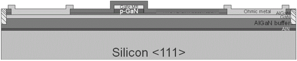
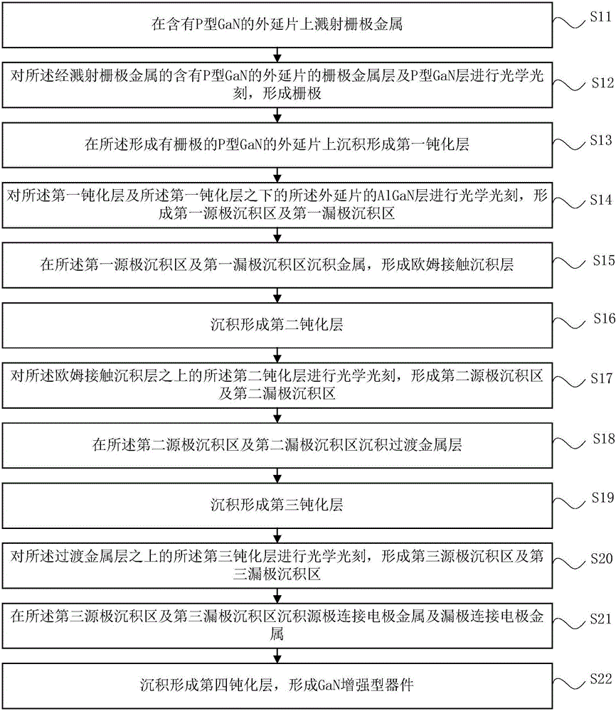
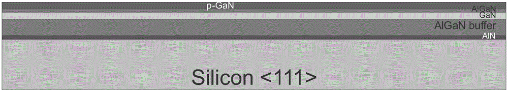
[0042] The invention provides a GaN enhanced device preparation method, such as figure 1 As shown, the method includes:

[0043] S11, sputtering gate metal on the epitaxial wafer containing P-type GaN;

[0044] S12. Perform optical lithography on the gate metal layer and the P-type GaN layer of the epitaxial wafer containing P-type GaN that...


PUM

PropertyMeasurementUnit
Thicknessaaaaaaaaaa

Abstract

The invention provides a fabrication method of a GaN enhancement device and the formed GaN enhancement device. According to the fabrication method of the GaN enhancement device, a gate, a source and a drain are formed on an epitaxial wafer containing P-type GaN by a process compatible with a complementary metal oxide semiconductor (CMOS) process. The fabrication process of the GaN enhancement device is compatible with the CMOS process, and thus, the production and the fabrication of an enhancement electronic power switch device in mass production and with low cost can be achieved.

Description

technical field [0001] The invention relates to the technical field of semiconductor manufacturing, in particular to a method for preparing a GaN enhanced device and the formed GaN enhanced device. Background technique [0002] Gallium nitride (GaN), as a wide bandgap compound semiconductor material device, has the characteristics of high output power and high temperature resistance. The research and application of GaN materials is the frontier and hot spot of global semiconductor research at present. It is a new semiconductor material for the development of microelectronic devices and optoelectronic devices. Together with semiconductor materials such as SIC and diamond, it is known as the successor to the first generation of Ge, Si Semiconductor materials, second-generation GaAs, and the third-generation semiconductor materials after InP compound semiconductor materials. [0003] With the development of high-voltage switches and high-speed radio frequency circuits, enhance...

Claims


Application Information

Patent Timeline
IPC IPC(8): H01L21/335H01L29/778
CPCH01L29/66462H01L29/7781
Inventor 刘新宇康玄武王鑫华黄森魏珂
Owner INST OF MICROELECTRONICS CHINESE ACAD OF SCI
Why Eureka
Try Eureka