
Two-level comparator

A comparator and input stage technology, applied in the electronic field, can solve the problems of large noise and large offset of the comparator, and achieve the effects of low noise, reduced offset and noise, and low timing requirements

Inactive Publication Date: 2016-12-07
UNIV OF ELECTRONICS SCI & TECH OF CHINA
View PDF4 Cites 10 Cited by
  • Summary
  • Abstract
  • Description
  • Claims
  • Application Information

AI Technical Summary

Problems solved by technology

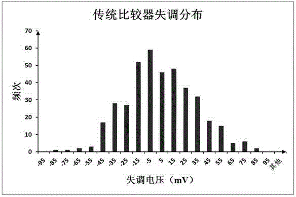
This traditional comparator is simple in structure and very fast, but has the following disadvantages: 1. The timing of the clock signal CLK and the inversion CLKB of the clock signal must be very accurate; 2. Since node X is at CLK=GND It has not been reset, resulting in relatively large offset of the comparator; 3. When the comparator enters the comparison stage, because the transistor MP5 enters the linear region, the noise is relatively large

Method used


Image

  • Two-level comparator
  • Two-level comparator
  • Two-level comparator

Examples


Embodiment Construction

[0016] The present invention will be further described below in conjunction with the accompanying drawings and specific embodiments.

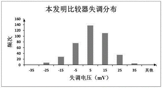
[0017] Aiming at the problems existing in the existing double-tailed comparator circuit, such as very precise timing requirements for the clock signal, relatively large comparator offset, and relatively large noise, the present invention proposes a two-stage comparator circuit. The specific circuit structure is as follows: figure 2 As shown, the two-stage comparator circuit includes an input stage and a latch stage, the input stage is composed of 3 NMOS transistors and 4 PMOS transistors, and the latch stage is composed of 6 NMOS transistors and 4 PMOS transistors; in the input stage The gates of the first NMOS transistor MN1, the third PMOS transistor MP3 and the fourth PMOS transistor MP4 are connected to the clock signal CLK; the drain of the first NMOS transistor MN1 is connected to the source of the second NMOS transistor MN2 and the sourc...


PUM


Abstract

The present invention relates to a two-level comparator circuit, belonging to the technical field of analog integrated circuits. The two-level comparator circuit comprises an input level and a latch level. The input level comprises a first N-channel metal oxide semiconductor (NMOS) transistor (MN1), a second NMOS transistor (MN2), a third NMOS transistor (MN3), a first p-channel metal oxide semiconductor (PMOS) transistor (MP1), a second PMOS transistor (MP2), a third PMOS transistor (MP3) and a fourth PMOS transistor (MP4). The latch level comprises a fourth NMOS transistor (MN4), a fifth NMOS transistor (MN5), a sixth NMOS transistor (MN6), a seventh NMOS transistor (MN7), an eighth NMOS transistor (MN8), a ninth NMOS transistor (MN9), a fifth PMOS transistor (MP5), a sixth PMOS transistor (MP6), a seventh PMOS transistor (MP7) and an eighth PMOS transistor (MP8). Due to reset of a node X+ and a node X- in a latch level circuit, circuit maladjustment and noise are lowered. A pair of cross-coupling transistors MP1 and MP2 is added in the input level circuit, so that the comparator has the characteristic of working at a high-speed. The two-level comparator is applicable to system circuits of high accuracy.

Description

technical field [0001] The invention belongs to the field of electronic technology, relates to an analog integrated circuit design technology, in particular to a high-speed comparator circuit with low noise and low offset. Background technique [0002] A comparator is a circuit that compares an analog voltage signal to a reference voltage. The traditional two-tailed comparator structure, such as figure 1 As shown, it consists of two stages, namely, the input stage and the latch stage, wherein the input stage is the first stage, and the latch stage is the second stage. The tail current of the input stage is controlled by the clock signal CLK, and the tail current of the latch stage is controlled by the inversion CLKB of the clock signal. When the clock signal CLK=GND, the comparator enters the reset phase (RESET). Transistors MP1 and MP2 pull up the output nodes DI+ and DI- of the first stage to the power supply voltage VDD, so that the transistors MN6 and MN7 are turned o...

Claims


Application Information

Patent Timeline
Patent Type & Authority Applications(China)
IPC IPC(8): H03K5/24
CPCH03K5/2481H03K5/249
Inventor 唐鹤印钰高昂何生生车来晟
Owner UNIV OF ELECTRONICS SCI & TECH OF CHINA
Learn More