printed wiring board

A technology of printed wiring boards and signal lines, which is applied in the fields of printed circuit, printed circuit, printed circuit manufacturing, etc., can solve the problems of insufficient transmission characteristics and high dielectric constant, and achieve the effect of high transmission characteristics and high wiring density

Active Publication Date: 2017-09-19
THE FUJIKURA CABLE WORKS LTD
View PDF6 Cites 0 Cited by
  • Summary
  • Abstract
  • Description
  • Claims
  • Application Information

AI Technical Summary

Problems solved by technology

[0004] However, epoxy-based thermosetting adhesives have a high dielectric constant, so there is a problem that the transmission characteristics at the time of high-frequency signal transmission are not sufficient.

Method used


Image

  • printed wiring board
  • printed wiring board
  • printed wiring board

Examples


Embodiment Construction

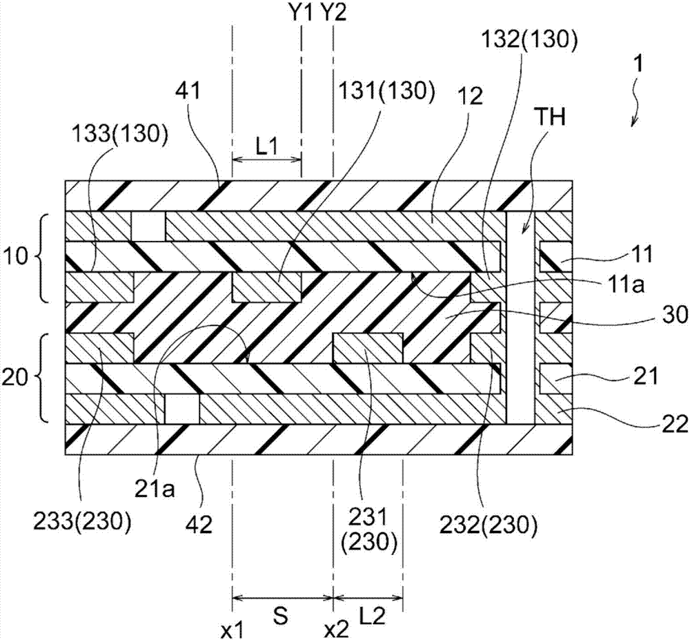
[0033] Hereinafter, an embodiment of the present invention will be described based on the drawings. In this embodiment, an example in which the printed wiring board 1 of the present invention is applied to a transmission line between circuits, between circuits and devices, or between connecting devices within a device will be described. The printed wiring board 1 of this embodiment is suitable for high-speed signal transmission, and can perform transmission based on various standards such as LVDS, MIPI, HDMI (registered trademark), and USB.

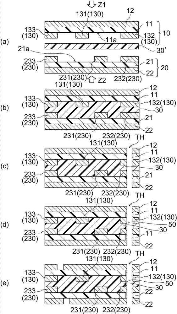
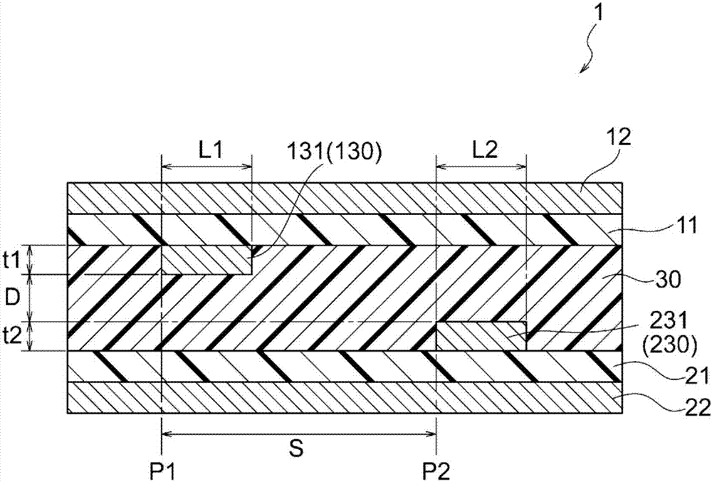
[0034] figure 1 It is a cross-sectional view of the printed wiring board 1 of this embodiment. Such as figure 1 As shown, the printed wiring board 1 of this embodiment has a laminated structure in which a first base material 10 and a second base material 20 are laminated. in figure 1 In the illustrated example, the first base material 10 is laminated on the upper side of the second base material 20, but it may be reversed.

[0035] The first...


PUM

PropertyMeasurementUnit
tensile strengthaaaaaaaaaa
glass transition temperatureaaaaaaaaaa
dielectric lossaaaaaaaaaa

Abstract

The printed wiring board of the present invention includes: a first insulating base material (11) formed of a liquid crystal polymer; a first signal line (131) formed on one main surface (11a) of the first insulating base material (11) ; The second insulating substrate (21), formed by liquid crystal polymer; The second signal line (231), formed on one of the second insulating substrate (21) along the extension direction of the first signal line (131) Main surface (21a); ​​and adhesive layer (30), one main surface (11a) of the first insulating base material (11) is bonded with one main surface (21a) of the second insulating base material (21) And it is made of modified polyphenylene ether. When the frequency of the signal transmitted by the first signal line and the above-mentioned second signal line is 2.5 GHz to 5.0 GHz, from the first signal line (131) along its width direction The distance from the position of one of the ends of the second signal line (231) to the position of one of the ends of the width direction of the second signal line (231), that is, the offset S is greater than that of the first signal line (131) The circuit width L1 is long and is not less than 130 μm and not more than 300 μm.

Description

Technical field [0001] The present invention relates to a printed wiring board. Background technique [0002] From the viewpoint of achieving high density and improving high-frequency transmission characteristics, there is known a flexible printed circuit in which an adhesive layer using an epoxy-based thermosetting adhesive is formed between laminated unit substrates (Patent Literature 1). [0003] Patent Document 1: JP 2012-243923 A [0004] However, the epoxy-based thermosetting adhesive material has a high dielectric constant, so there is a problem that the transmission characteristics during high-frequency signal transmission are insufficient. Summary of the invention [0005] The problem to be solved by the present invention is to provide a printed wiring board with high transmission characteristics and high wiring density during high-frequency signal transmission. [0006] The present invention provides a printed wiring board characterized by comprising: a first insulating bas...

Claims


Application Information

Patent Timeline
Patent Type & Authority Patents(China)
IPC IPC(8): H05K3/46C09J171/12H01P3/02H01P3/08H05K1/02
CPCH01P3/088H01P11/003H05K1/0228H05K3/429H05K3/4635H05K2201/0141H05K2203/061C09J171/12H01P3/02H01P3/08H05K1/024H05K3/4676H01P3/085H05K1/0225H05K1/0237H05K1/03
Inventor 小松尚美
Owner THE FUJIKURA CABLE WORKS LTD
Why Eureka
Try Eureka