Mask slice graphic structure and manufacturing method of semiconductor chip

A pattern structure and mask technology, applied in the direction of semiconductor devices, semiconductor/solid-state device components, electric solid-state devices, etc., can solve the problems of inability, the cutting line cannot have any graphics and metal, and the process inspection mark pattern cannot be placed. Achieve the effect of avoiding stress damage, ensuring inspection and electrical performance testing, and avoiding wear and tear

Active Publication Date: 2016-12-21
SEMICON MFG INT (SHANGHAI) CORP
View PDF3 Cites 1 Cited by
  • Summary
  • Abstract
  • Description
  • Claims
  • Application Information

AI Technical Summary

Problems solved by technology

However, the inventor found that the DRIE cutting technology requires that the cutting line should not have any graphics and metal, and the graphics of process inspection marks and test keys cannot be placed, so it cannot be effectively promoted

Method used


Image

  • Mask slice graphic structure and manufacturing method of semiconductor chip
  • Mask slice graphic structure and manufacturing method of semiconductor chip
  • Mask slice graphic structure and manufacturing method of semiconductor chip

Examples


Embodiment Construction

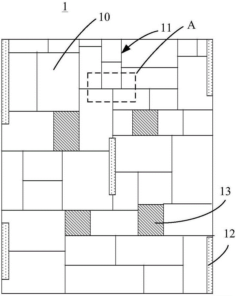
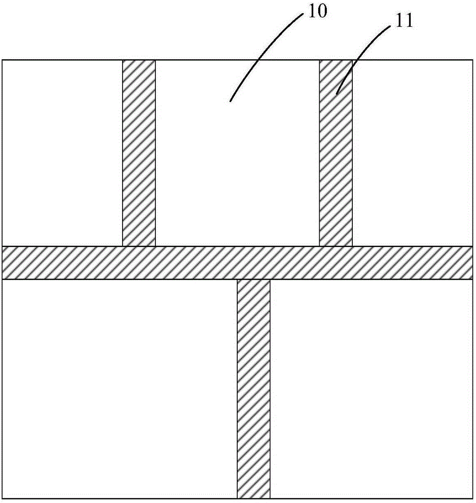
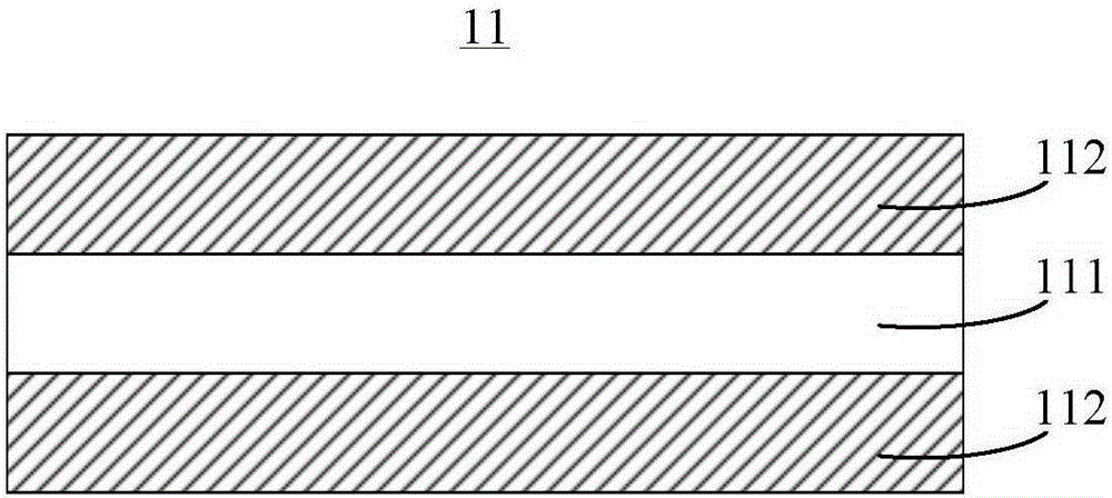
[0030] The mask pattern structure and semiconductor chip manufacturing method of the present invention will be described in more detail below in conjunction with schematic diagrams, wherein a preferred embodiment of the present invention is shown, it should be understood that those skilled in the art can modify the present invention described here, and still The advantageous effects of the present invention are realized. Therefore, the following description should be understood as the broad knowledge of those skilled in the art, but not as a limitation of the present invention.

[0031] In the following paragraphs the invention is described more specifically by way of example with reference to the accompanying drawings. Advantages and features of the present invention will be apparent from the following description and claims. It should be noted that all the drawings are in a very simplified form and use imprecise scales, and are only used to facilitate and clearly assist the...


PUM


Abstract

The invention relates to a mask slice graphic structure and a manufacturing method of a semiconductor chip. The mask slice graphic structure comprises chip unit graphs, adjacent chip unit graphs are separated from each other by a cutting channel graph, the cutting channel graph comprises an etching band graph and vacant areas arranged at the two sides of the etching band graph, and the etching band graph and the vacant areas are arranged along the width direction of the cutting channel graph; and the mask slice graphic structure also comprises multiple process detecting areas which are arranged in the surrounding of at least one chip unit graph and a test button area which is arranged in the chip unit graph. Compared with the prior art, DRIE technology, basically instead of an electric saw, can be utilized to cut the chip, wearing of the electric saw during packaging cutting is reduced and even avoided, and waste of chips is reduced as possible.

Description

technical field [0001] The invention relates to the technical field of semiconductors, in particular to a pattern structure of a mask plate and a method for manufacturing a semiconductor chip. Background technique [0002] MPW (Multi-Project Wafer, multi-project wafer) is to put multiple integrated circuit designs with the same process on the same wafer, and share the cost of tape-out according to the area, so as to reduce development costs and new product development risks, and reduce the risk of small and medium-sized wafers. The threshold for integrated circuit design companies at the start, to avoid the serious waste of resources caused by a single test tape-out. [0003] MPW needs to perform wafer thinning, scribing (cutting), and testing after chip manufacturing after the mask plate is made from the foundry line. [0004] The current mainstream cutting method is die saw, that is, using a chainsaw to cut along the dicing line of each chip. This method has the advantage...

Claims


Application Information

Patent Timeline
Patent Type & Authority Applications(China)
IPC IPC(8): H01L27/02H01L23/544
Inventor 张士健陆晓锋戴文旗徐佳明李晨
Owner SEMICON MFG INT (SHANGHAI) CORP
Why Eureka
Try Eureka