CSP light source and manufacturing method thereof

A manufacturing method and light source technology, applied in the field of CSP light source and its manufacturing, can solve the problems of insufficient central brightness of the light source, low adhesive force, and reduced luminous flux of the light source, so as to reduce the loss of luminous flux, increase the central light intensity, and improve the luminous efficiency. Effect

Inactive Publication Date: 2016-12-21
江西兆驰光元科技股份有限公司
View PDF8 Cites 7 Cited by
  • Summary
  • Abstract
  • Description
  • Claims
  • Application Information

AI Technical Summary

Problems solved by technology

[0005] (1) Since all five sides emit light, the center brightness of the light source is insufficient, so it cannot be applied to areas with high center brightness requirements such as mobile phone flashlights;
[0006] (2) The fluorescent glue on the bottom periphery of the light-emitting chip is excited by the blue light emitted by the light-emitting chip, and the light generated will be emitted from the lower part. This part of the light will usually be rapidly attenuated due to multiple refractions and reflections, resulting in the loss of the light source. The overall luminous flux is reduced, and the utilization rate of light is not high;
[0008] (4) Ordinary five-sided light-emitting CSP light source, the bonding of the light-emitting chip and the fluorescent colloid is based on the inherent adhesive properties of the colloid. This adhesive force is very small, making this CSP light source prone to fluorescence during use. The colloid is detached from the light-emitting chip, resulting in the failure of the light source

Method used


Image

  • CSP light source and manufacturing method thereof
  • CSP light source and manufacturing method thereof
  • CSP light source and manufacturing method thereof

Examples


Embodiment Construction

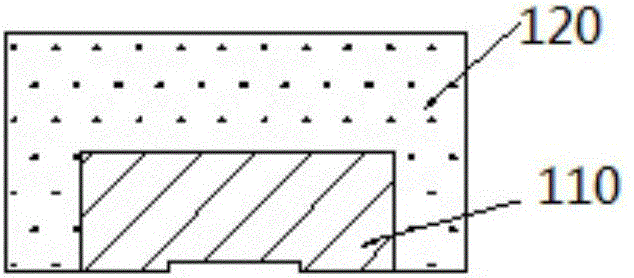
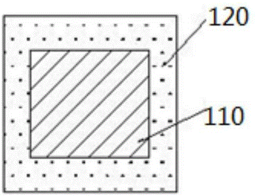
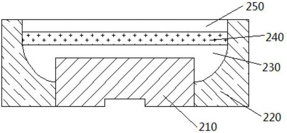
[0034] see image 3 , in this embodiment, the CSP light source of the present invention includes a light emitting chip 210, a first transparent silica gel layer 230, a fluorescent colloid layer 240, and a second transparent silica gel layer 250 arranged sequentially from bottom to top. The four-layer structure of the transparent silicone layer 230 , the fluorescent colloid layer 240 , and the second transparent silicone layer 250 is surrounded by an outer colloid layer 220 with reflective properties.

[0035] The outer colloidal layer 220 is a white colloidal layer with high reflection performance and high tensile strength.

[0036] Specifically, the outer colloid layer 220 is combined with the light-emitting chip 210 to form a bowl-like structure. The bottom of the light emitting chip 210 and the electrodes provided on the bottom are exposed.

[0037] As an alternative embodiment, a fluorescent colloid layer may be provided on the light-emitting chip 210 , and an outer coll...


PUM


Abstract

The invention provides a CSP light source and a manufacturing method thereof, which includes a light-emitting chip, on which a fluorescent colloid layer is arranged, and around the light-emitting chip and the fluorescent colloid layer are surrounded by an outer colloid layer with reflective properties. The manufacturing method of the CSP light source of the present invention comprises: (1) pasting the transparent adhesive film on the carrier plate; (2) pasting the fluorescent adhesive film on the transparent adhesive film; (3) coating the liquid transparent silica gel film on the fluorescent adhesive film ; (4) Mount the light-emitting chip on the liquid transparent silicone film and cure it by heating; (5) Cut out a channel with a specific width along the edge of the transparent silicone layer next to the light-emitting chip; (6) In the cut out channel Coating with reflective coating and curing. The CSP light source of the present invention is equipped with an outsourcing colloidal layer with reflective properties, forming a light-gathering structure, which is beneficial to light-gathering, reduces luminous flux loss, improves the overall brightness of the light source, and increases the central light intensity; and because the fluorescent glue layer is located in the blue light Right above the light-emitting chip, the phosphor powder can be fully excited, which improves the light extraction efficiency of the light source.

Description

【Technical field】 [0001] The invention relates to the lighting field, in particular to a CSP light source and a manufacturing method thereof. 【Background technique】 [0002] The existing common five-sided light-emitting CSP light source (Chip Scale Package, chip scale package) structure is as follows figure 1 , figure 2 As shown, it consists of a light-emitting chip 110 in the middle and a fluorescent colloid 120 surrounding the light-emitting chip from above and around. Among them, the light-emitting chip 110 is a flip-chip with electrodes located at the bottom of the chip, so that the light source can be directly welded to the application end substrate, eliminating the need for a wire bonding process, and at the same time avoiding the reliability problem that the traditional SMD light source is easy to disconnect and die; the fluorescent glue is made of It is made by mixing transparent silica gel, fluorescent powder and auxiliary additives. [0003] The existing common...

Claims


Application Information

Patent Timeline
Patent Type & Authority Applications(China)
IPC IPC(8): H01L33/00H01L33/50H01L33/52
CPCH01L33/52H01L33/005H01L33/502
Inventor 周波何至年唐其勇
Owner 江西兆驰光元科技股份有限公司
Why Eureka
Try Eureka